EZ-USB FX3 Technical Reference Manual, Document Number: 001-76074 Rev. *F 29
Introduction to EZ-USB FX3
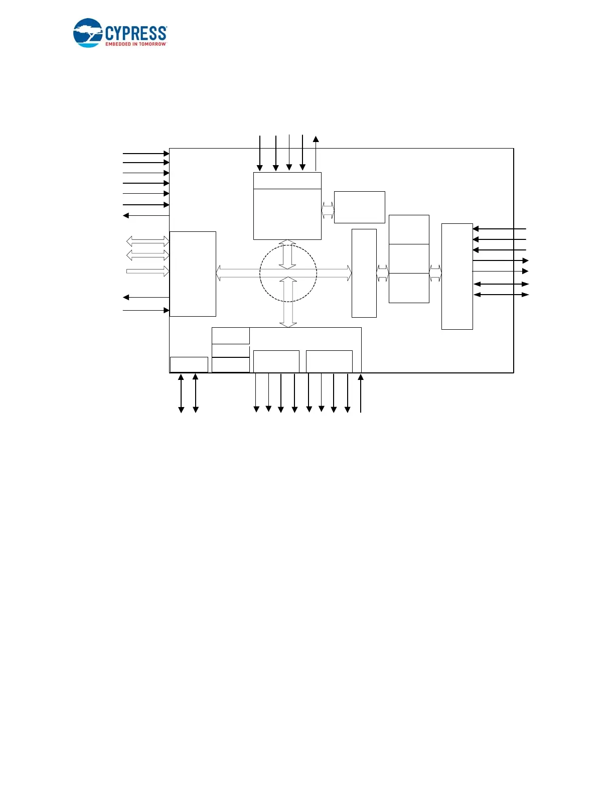
1.3.2 FX3S Block Diagram
Figure 1-7. FX3S Block Diagram
Note: For more details on pin mapping and their descriptions, refer to FX3 and FX3S datasheets.
1.4 Functional Overview
1.4.1 CPU
FX3 has an on-chip 32-bit, 200-MHz ARM926EJ-S core CPU. The core has direct access to 16 KB of instruction tightly
coupled memory (TCM) and 8 KB of data TCM. The ARM926EJ-S processor also has associated instruction cache (I-cache)
and data cache (D-cache) memories. Both the instruction and data caches are 8 KB.
FX3 integrates 512 KB or 256 KB (depending on the part number) of embedded SRAM for storing code and data. The
ARM926EJ-S core provides a JTAG interface for firmware debugging.
FX3 interrupts are managed through the standard ARM PrimeCell Vectored Interrupt Controller (PL192) block. This interrupt
controller provides vectored interrupt support with configurable priorities for all interrupt sources.
Examples of the FX3 firmware are available with the Cypress EZ-USB FX3 Development Kit.
For more information about the CPU subsystem, refer to the FX3 CPU Subsystem chapter on page 34.
For more information about the memory map, refer to the Memory and System Interconnect chapter on page 44.
32
EPs
GPIF II
SS
Peripheral
HS/FS/LS
OTGHost
JTAG
UART
SPI
CTL[15:0]
INT#
RESET#
TDI
TDO
TRST#
TMS
TCK
DQ[15:0]
PMODE[2:0]
SSRX +
SSRX -
SSTX +
SSTX -
D +
D -
FSLC[0]
FSLC[1]
FSLC[2]
CLKIN
CLKIN_32
XTALIN
XTALOUT
OTG_ID
I2S
I2C
SRAM
(512kB/256kB)
ARM9
USB
HS/FS
Peripheral
DMA
Interconnect
I2C_SCL
I2C_SDA
S1_CMD
S1_WP
S1_D[7:0]
SD/MMC controller
S0-port S1-port
S1_CLK
S0_CLK
S0_CMD
S0_WP
S0_D[7:0]
S0S1_INS

 Loading...


