EZ-USB FX3 Technical Reference Manual, Document Number: 001-76074 Rev. *F 60
FX3 DMA Subsystem
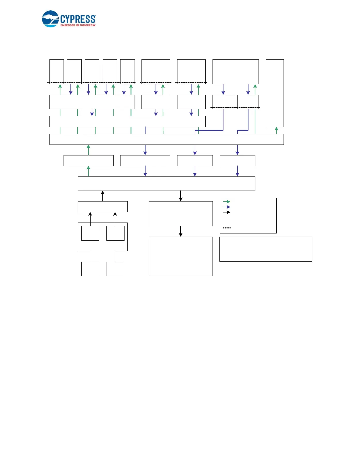
Figure 5-2. Distributed DMA Controllers
5.5 DMA Subsystem Components
5.5.1 Clocking
The FX3 DMA subsystem runs on an internal DMA bus clock, dma_bus_clk_i, that is divided down from the CPU clock. The
DMA bus clock divider value is determined by the DMA_DIV field of GCTL_CPU_CLK_CFG, as shown below:
DMA Bus clock divider = (GCTL_CPU_CLK_CFG.DMA_DIV + 1)
See GCTL_CPU_CLK_CFG register on page 260
Divide by 1 (i.e. GCTL_CPU_CLK_CFG.DMA_DIV = 0) is illegal and will result in undefined behavior. Thus, the range of
allowed divider values is 2 to 16 (GCTL_CPU_CLK_CFG.DMA_DIV => 1 to 15).
A typical dma_bus_clk_i frequency is set to one-half the CPU clock during device initialization. For example, if the CPU clock
is set to 192 MHz, the register setting GCTL_CPU_CLK_CFG.DMA_DIV=1 (divider = 2) will result in a 96 MHz of
dma_bus_clk_i frequency. Table 5 - 1 summarizes the DMA clock information.
WR DMA
Adapter
SIB
High Speed System Interconnect
(Accelerated AHB, 2 x 128b x 200MHz, 3.2+3.2GB/s)
Main System SRAM
Instances Array
512KB, 128b, 200MHz, 0ws
3.2GB/s
ARM926EJ-S
Instr
TCM
(16KB)
Data
TCM
(8KB)
ARM TCM
200MHz x 32 b
Instr
Cache
(8KB)
Data
Cache
(8KB)
Memory Controller
3.2GB/s
(Up to 100 % Utilization)
AHB Bridge
(Synchronous)
ARM TCM
200MHz x 32b
2x AHB
200 MHz x 32b
1,8cy bursts 1, 4,8cy bursts
1cy accesses
Acc AHB
2x 200MHz x 128b
1cy bursts
Acc AHB
2x 200 M Hz x 128b
1cy bursts
1cy accesses
UIBPIB
UART
AHB Bridge
(Synchronous)
I2SI2C SPIGPIO
SRAM
200MHz x 128b
Main DMA Interconnect
(Accelerated AHB, 2x 100MHz x 64b, 800+800MB/s)
DMA
Adapter
DMA
Adapter
DMA
Adapter
AHB Bridge
(Synchronous)
AHB Bridge
(Synchronous)
RD DMA
Adapter
Acc AHB (RD only)
200 MHz x 128 b
Acc AHB
2x 200 M Hz x 128 b
Acc AHB
2x 200M Hz x 128b
1cy bursts1cy bursts1cy bursts
AHB
100MHz x 32b
1cy bursts
Acc AHB
2x 100 M Hz x 64b
2cy bursts
Acc AHB (RD only)
100 MHz x 64 b
2cy bursts
Register Access
DMA Traffic
Registers & DMA
(Arrow points mast ter -to-slave)
Denotes async clock crossing
fr om bus to core clock domains
Clock Sources :
Bus /CPU SysPLL Locked 1 :1 or 1: 2, typ 100 /200 MHz
SIB /PIB /LPP SysPLL Indivi dual Di vi ers
Async coupled to bus / cpu
UIB USB 2PLL 120 M Hz ( Adapter ), 30 M Hz (SIE /TP )
USB 3PLL 125 M Hz ( SuperSpeed mode only )
GCTL
AHB Bridge
(Synchronous)
AHB ( WR only)
200 M Hz x 128 b
1cy bursts
MMIO Interconnect
(AHB, 100MHz x 32b, ~50-100MB/s)
Acc AHB (WR only)
100 M Hz x 64 b
2cy bursts

 Loading...


