EZ-USB FX3 Technical Reference Manual, Document Number: 001-76074 Rev. *F 623
SCK_INTR
0x00
10.26 DMA Adapter Global Registers
Each functional block (LPP, PIB, UIB, and UIBIN) has its own set of DMA registers that use the offset address of that block.
Table 10-4 shows the offset address for each block.
Each functional block has more than one DMA and each DMA has the same set of DMA Socket registers. The offset of each
DMA Socket register set is 0x80 (that is, the offset of DMA #0 is 0, DMA #1 is 0x80, DMA #2 is 0x100, and so on). The
address of a DMA Socket register can be calculated as:
functional block address + DMA # * 0x80 + register address
For example, the address of the ADAPTER_DEBUG register of DMA #2 in the UIB functional block can be calculated as:
0xE003FF00 + 2 (DMA #2) * 80 + 0xF4 = 0xE003FF00 + 0x100 + 0xF4 = 0xE00400F4.
10.26.1 SCK_INTR
Socket Interrupt Request Register
continued on next page
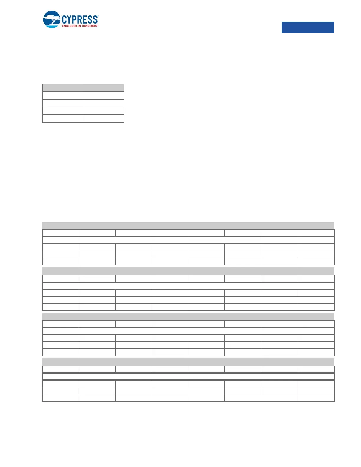
Table 10-4. Offset Addresses
Functional Block Offset Address
LPP 0xE000FF00
PIB 0xE001FF00
UIB 0xE003FF00
UIBIN 0xE00FF000
SCK_INTR Socket Interrupt Request Register 0x00
b255 b254 b253 b252 b251 b250 b249 b248
SCKINTR[255:248]
RRRRRRRR
WWWWWWWW
00000000
SCK_INTR Socket Interrupt Request Register
b247 b246 b245 b244 b243 b243 b241 b240
SCKINTR[247:240]
RRRRRRRR
WWWWWWWW
00000000
SCK_INTR Socket Interrupt Request Register
b239 b238 b237 b236 b235 b234 b233 b232
SCKINTR[239:232]
RRRRRRRR
WWWWWWWW
00000000
SCK_INTR Socket Interrupt Request Register
b231 b230 b229 b228 b227 b226 b225 b224
SCKINTR[231:224]
RRRRRRRR
WWWWWWWW
00000000
 Loading...


