EZ-USB FX3 Technical Reference Manual, Document Number: 001-76074 Rev. *F 176
Low Performance Peripherals (LPP)
■ Provides the Chip Select (CS#) signal
■ Provides SPI clock up to 33 MHz
■ FX3 can boot from SPI flash/ EEPROM (refer to AN76405 - EZ-USB FX3 Boot Options for more information)
8.3.2 SPI Interface Overview
The SPI bus is a synchronous serial data link interface, named by Motorola, which operates in full duplex mode. Devices
communicate in master/slave mode where the master device initiates the data frame and provides the clock. Multiple slave
devices are allowed with individual slave select (chip select) lines. Sometimes SPI is called a four-wire serial bus, in contrast
to three-, two-, and one-wire serial buses.
During an SPI transmission, data is transmitted (shifted out serially) and received (shifted in serially) simultaneously. The
serial clock (SCK) synchronizes the shifting and sampling of information on the two serial data lines. A slave select line allows
an individual slave SPI device to be selected. Slave devices that are not selected do not interfere with SPI bus activities.
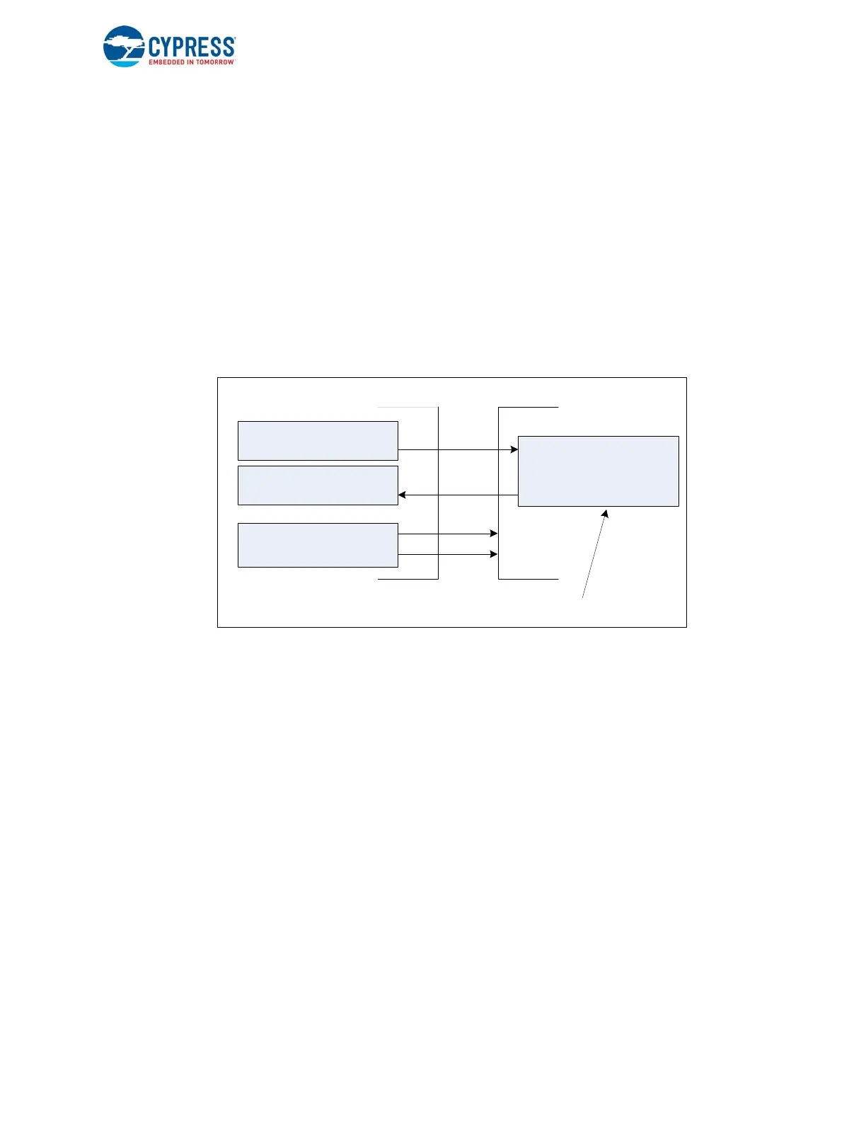
Figure 8-3. SPI Bus
The FX3 SPI block operates in master mode and facilitates standard full-duplex synchronous transfers using the master out,
slave in (MOSI), master in, slave out (MISO), serial interface clock (SCK), and slave select (SSN) pins. The roles of the four
SPI interface pins are as follows:
■ SCK: As the SPI master, FX3 provides this clock. The FX3 SPI interface clock can run up to 33 MHz. This clock is gated
so that start and stop of transaction can be signaled in conjunction with the SS line. Eight clock cycles are generated on
this line per transfer.
■ SSN: As the SPI master, FX3 drives the slave select line in a mode-dependent fashion along with SCK to signal the start
of the transaction. Depending upon mode, a slave can remain selected for multiple 8-bit transactions (based on Clock
Phase (CPHA) configuration), has to toggle between transactions, or can be firmware controlled. FX3 also supports firm-
ware control operation of the SSN line. It has a provision to drive SSN signal with a programmable lead and lag with
respect to SCK at the start and end of transmission.
■ MOSI: FX3 drives serial data on the MOSI line. Data can be driven on the positive or negative edge of SCK selected by a
configuration bit. The selected slave samples the data on the negative or positive edges respectively.
■ MISO: FX3 samples serial data on the MISO line. Data can be driven by the selected slave on the positive or negative
edge of SCK governed by a configuration bit. FX3 samples the data on the negative or positive edge respectively.
The SPI block supports single and burst (DMA) data transfers. The SPI transmit and SPI receive blocks can be enabled
independently using the TX_ENABLE/RX_ENABLE register settings. Independent shift registers are used for the transmit
and receive paths. The shift register length can be set to values between 4 and 32 bits. By default, the TX and RX registers
shift data to the left. This can be reversed, if necessary.
TX SHIFT REGISTER
RX SHIFT REGISTER
SHIFT REGISTER
MOSI
MISO
SCK
SSN
Controls
Master SPI
Slave SPI
Shift register can be single or two
(as shown in Master)

 Loading...


