EZ-USB FX3 Technical Reference Manual, Document Number: 001-76074 Rev. *F 562
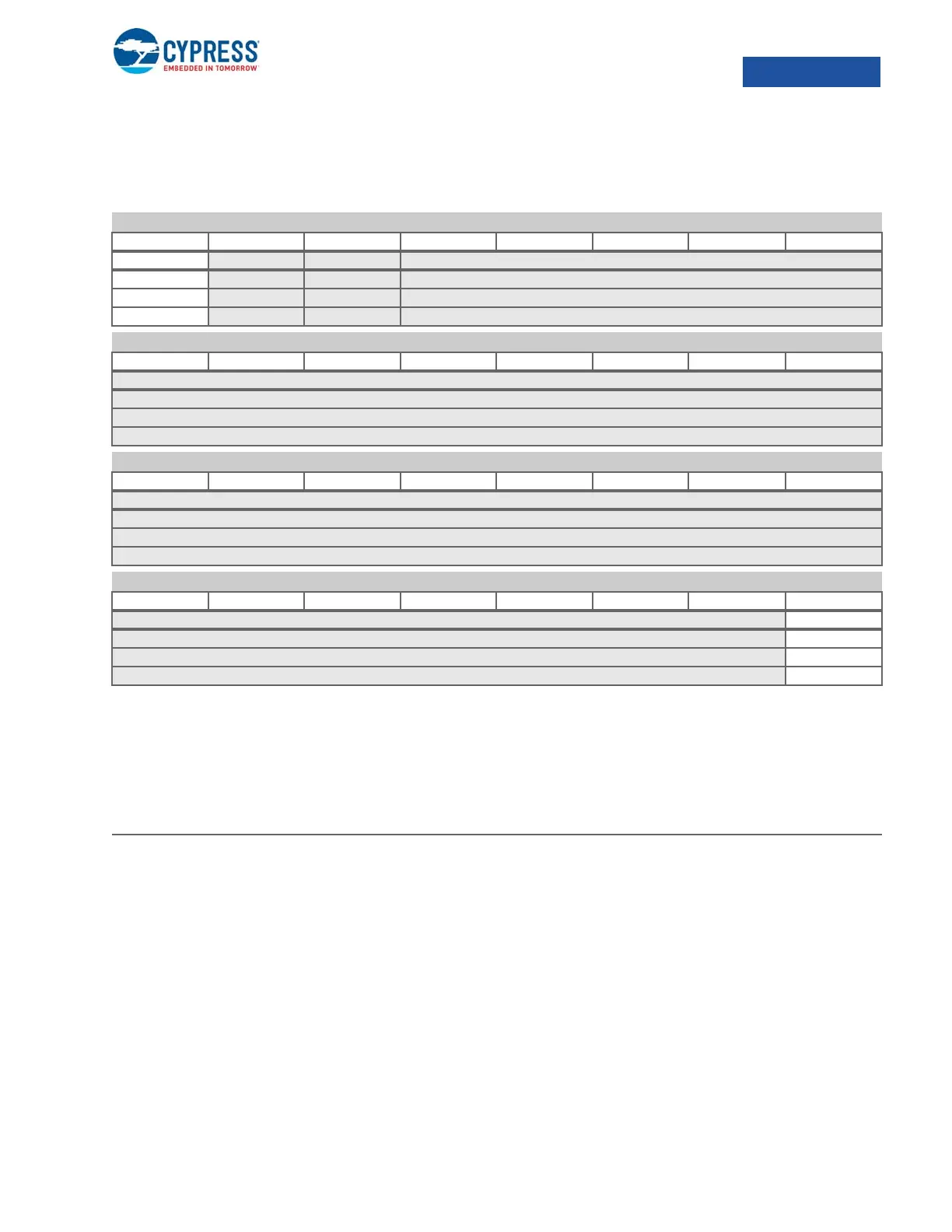
I2C_POWER
0xE00007F4
10.19.18 I2C_POWER
Power, Clock, and Reset Control Register
Every low performance peripheral IP block will implement a few MMIO registers at a fixed offset in its MMIO to space that
identify the block and control its power/clock/reset state. These registers are located in the CPU/Interconnect power and clock
domains and are accessible even when power/clock of the block is switched off.
31 RESETN Active LOW reset signal for all logic in the block. Note that reset is active on all flops in the block
when either system reset is asserted (RESET# pin or SYSTEM_POWER.RESETN is asserted) or
this signal is active.
After setting this bit to 1, firmware will poll and wait for the ‘active’ bit to assert. Reading ‘1’ from
‘resetn’ does not indicate the block is out of reset – this may take some time depending on initializa-
tion tasks and clock frequencies.
This bit must be asserted ('0') for at least 10 µs for effective reset.
0 ACTIVE For blocks that must perform initialization after reset before becoming operational, this signal will
remain deasserted until initialization is complete. In other words reading active=1 indicates block is
initialized and ready for operation.
I2C_POWER Power, Clock, and Reset Control 0xE00007F4
b31 b30 b29 b28 b27 b26 b25 b24
RESETN
R/W
R
0
I2C_POWER Power, Clock, and Reset Control
b23 b22 b21 b20 b19 b18 b17 b16
I2C_POWER Power, Clock, and Reset Control
b15 b14 b13 b12 b11 b10 b9 b8
I2C_POWER Power, Clock, and Reset Control
b7 b6 b5 b4 b3 b2 b1 b0
ACTIVE
R
W
0
Bit Name Description

 Loading...


