EZ-USB FX3 Technical Reference Manual, Document Number: 001-76074 Rev. *F 229
Registers
10.2 Register Conventions
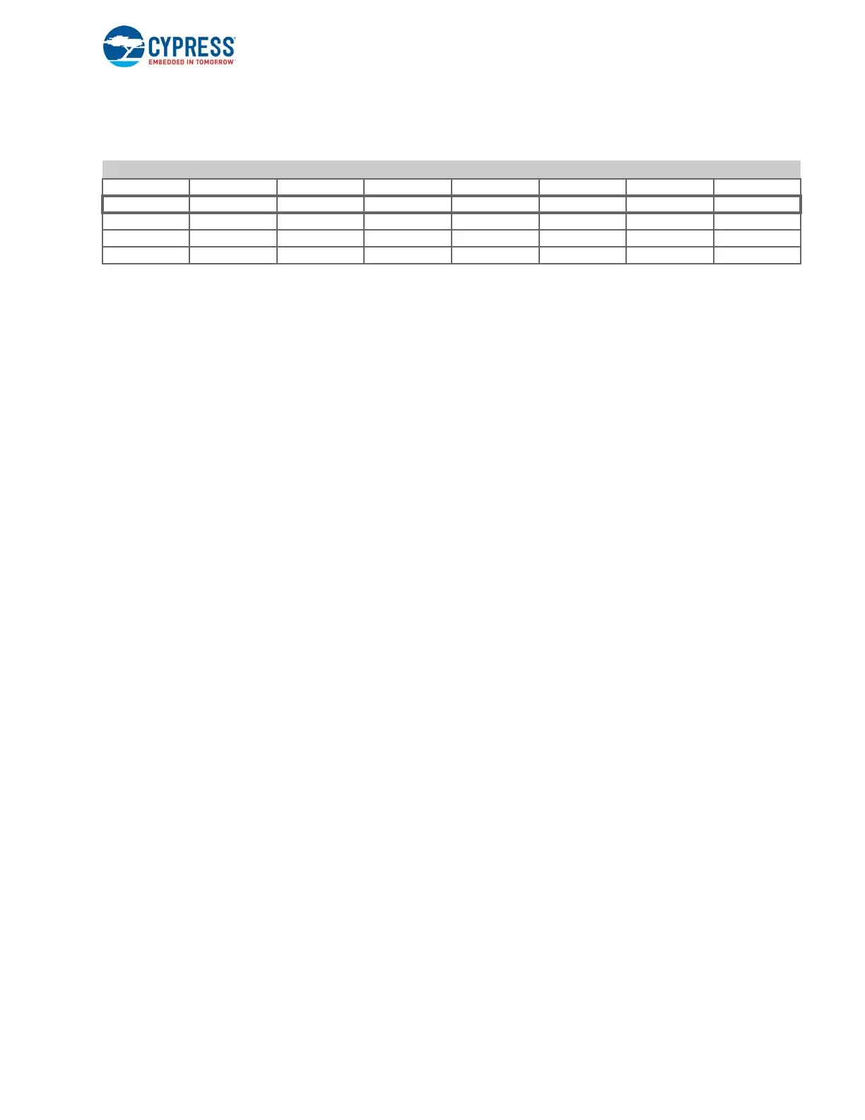
The register table above illustrates the register description format used in this chapter.
■ The top line shows the register name, functional description, and address in the memory.
■ The second line shows the bit position in the register.
■ The third line shows the field name of the corresponding bit(s) in the register.
■ The fourth line shows SW CPU accessibility: R(ead), W(rite), W0C (write 0 to clear), W1S (write 1 to set), or R/W.
■ The fifth line shows HW CPU accessibility: R(ead), W(rite), W0C (write 0 to clear), W1S (write 1 to set), or R/W.
■ The sixth line shows the default value. These values apply after a hard reset (refer to 4.3.3 Reset on page 57). When a
default value extends across bytes, the borders between the bytes is a lighter line.
■ Gray, empty cells indicate reserved bits. Do not read from or write to these bits.
Register Name Register Function Address
b7 b6 b5 b4 b3 b2 b1 b0
bitname bitname bitname bitname bitname bitname bitname bitname
SW R, W access SW R, W access SW R, W access SW R, W access SW R, W access SW R, W access SW R, W access SW R, W access
HW R, W access HW R, W access HW R, W access HW R, W access HW R, W access HW R, W access HW R, W access HW R, W access
Default val Default val Default val Default val Default val Default val Default val Default val

 Loading...


