EZ-USB FX3 Technical Reference Manual, Document Number: 001-76074 Rev. *F 61
FX3 DMA Subsystem
Note: The maximum DMA clock frequency is half of the CPU clock frequency, as the minimum allowed divider value is '2'.
Therefore, reducing the CPU clock frequency will result in reducing the DMA clock frequency and limit system performance.
The default clock settings for FX3 are:
■ CPU clock = System clock / 2
■ DMA clock = CPU clock / 2
It is recommended that the default clock settings be retained in all cases.
Table 5-1. DMA Clock
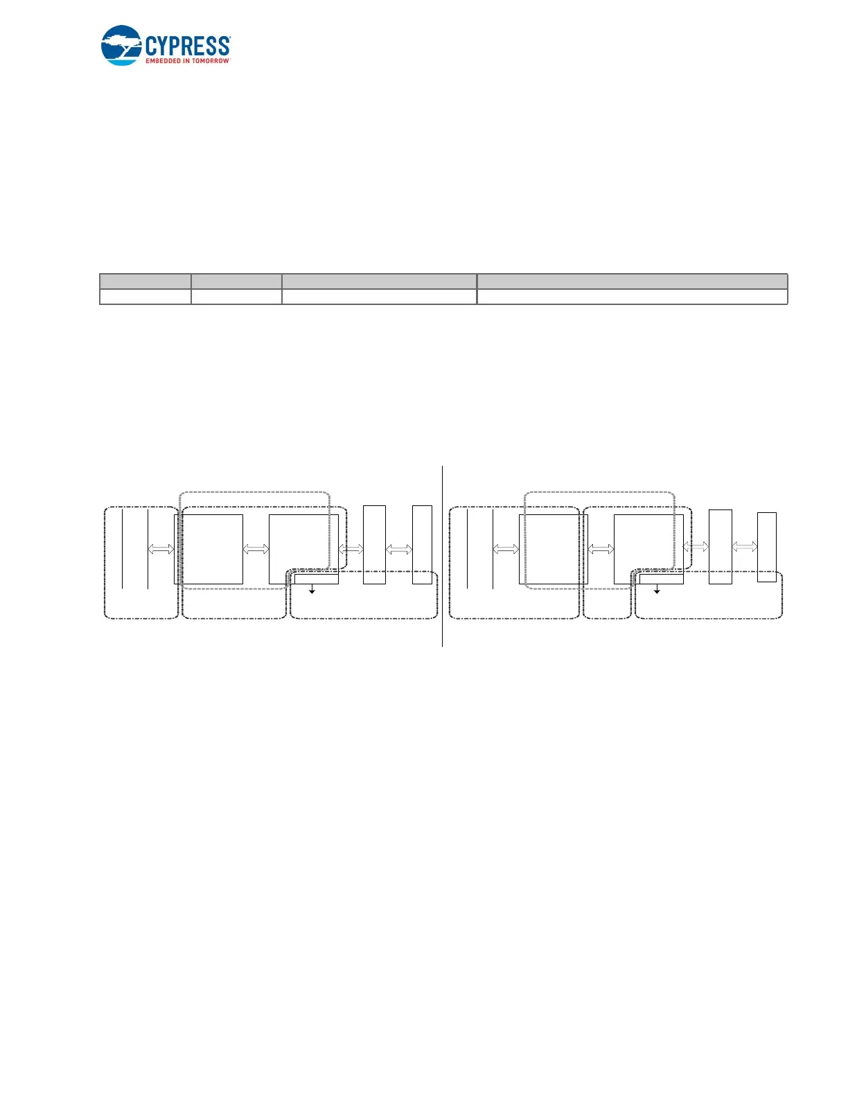
The CPU, DMA, and MMIO clock domains are synchronous to each other. However, every peripheral assumes its core clock
to be fully asynchronous from other peripheral core clocks, the computing clock, or the wakeup clock.
If the core (peripheral) clock is faster than the bus clock, the DMA adapter for the block runs in the core clock domain and the
DMA adapter reconciles the clocks on its interconnect side. If the core clock is slower than the bus clock, the DMA adapter for
that block runs in the bus clock domain and the DMA adapter reconciles the clocks on its core IP side. This is shown in
Figure 5-3.
Figure 5-3. DMA Adapter Clock
5.5.2 Descriptors Buffers, and Sockets
DMA descriptors are DMA instructions in a set of registers allocated in the FX3 RAM. A DMA descriptor holds information
about the address and size of the DMA buffer as well as pointers to the next DMA Descriptor. These pointers create DMA
descriptor chains. Descriptors enable the synchronization between sockets as described below.
A DMA buffer is a section of RAM used for intermediate storage of data transferred through the FX3 device. DMA buffers are
allocated from the system RAM by the FX3 firmware; their addresses are stored as part of DMA descriptors. Every buffer
created in the system memory has a descriptor associated with it that contains buffer information such as its address, empty/
full status, and the next buffer/descriptor in the chain.
A socket is a point of connection between a peripheral hardware block and the FX3 RAM. Each peripheral hardware block on
FX3 such as USB, GPIF, UART, and SPI has a fixed number of sockets associated with it. The number of parallel data
channels through a peripheral is equal to the number of its sockets. The socket implementation includes a set of registers that
point to the active DMA descriptor and the enable or flag interrupts associated with the socket. Sockets can directly signal
each other through events or they can signal the FX3 CPU via interrupts. This signaling is configured by firmware.
5.5.3 DMA Descriptors
Descriptors are data structures that keep track of the resources (memory buffers and sockets) used for a DMA transfer. This
data structure is directly interpreted by the DMA hardware on FX3, and has to be located in a specific memory region of the
Domain Typ/ Max Freq Configuration Register Source Description
dma_bus_clk_i 100 MHz GCTL_CPU_CLK_CFG.DMA_DIV DMA access clock
Core Logic
Block XYZ
I/ O
Pads
DMA / Bus
Adapter
Wake Up
Logic
I/O
Matrix
System
Interconnects
Block XYZ
Clock Domain
Always - On
Clock / Power / Reset Domain
Processor / Bus
Clock Domain
wakeup
Block XYZ Power Domain
Core Logic
Block XYZ
I/ O
Pads
DMA / Bus
Adapter
Wake Up
Logic
I/O
Matrix
System
Interconnects
Block
XYZ
Clock
Domain
Always - On
Clock / Power / Reset Domain
Processor / Bus
Clock Domain
wakeup
Block XYZ Power Domain
(a) Core Clock >Bus clock
(b) Bus clock>Core Clock

 Loading...


