EZ-USB FX3 Technical Reference Manual, Document Number: 001-76074 Rev. *F 48
Memory and System Interconnect
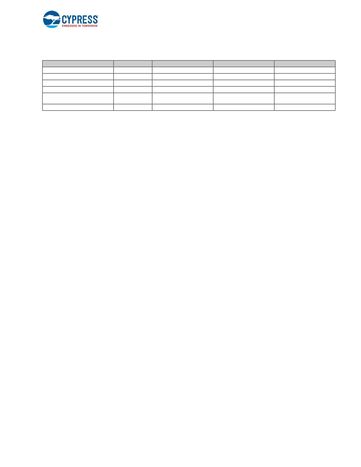
Table 3-1. State of FX3 Blocks in Low-Power Modes
The device supports two variants of suspend modes: L1 and L2. All the device blocks will be in the clock gated state in the L1
mode. This mode can be entered when the USB connection to the FX3 device has been suspended by the host, and the
device should be configured to wake up on any USB bus activity.
The USB block is powered off in the L2 suspend mode. This mode can be entered only if the VBus input to the device is
turned off. The device can be configured to wake up when the VBus input is detected.
In the standby mode, most of the blocks on the device are powered off. Only the system RAM and the logic required to detect
wakeup requests are left powered on. Since the CPU as well as all the blocks including USB are powered off in this mode,
firmware operation after wakeup is similar to that on a warm reset of the device.
3.3.4 Cache Operations
The FX3 device has dedicated instruction and data caches that improve access latencies to the SYSTEM RAM region. The
caches are not used for TCM, MMIO, and VIC access. TCMs guarantee single-cycle access for both instructions and data,
and they do not require a cache. The MMIO and VIC registers need to be updated atomically, and they are configured as not
cacheable.
The ARM9 architecture supports the following cache operations:
■ Flushing the entire I-cache or D-cache
■ Cleaning (writing back to memory) the entire D-cache
■ Flushing (evicting) a memory region from the I-cache or D-cache
■ Cleaning (writing back to memory) a memory region from the D-cache
■ Loading a specific memory region into the I-cache or D-cache
Refer to the ARM926EJ-S Technical Reference Manual or the ARM System Developer's Guide for details on how to perform
these operations.
Enabling the instruction cache is recommended for all FX3 applications. Enabling the data cache helps improve performance
in applications where the FX3 CPU performs data manipulations.
3.3.4.1 Cache Coherency
Almost all FX3 applications involve transferring data in or out through one or more of the device interfaces. All these data
transfers are achieved through the distributed DMA fabric on the device and make use of a part of the system RAM for
buffering.
As the system RAM is used for DMA buffers as well as for code and data storage, there is a possibility of cache/memory
corruption when the D-cache is enabled. The firmware application needs to avoid this possibility using the following
guidelines. These steps are handled by the FX3 firmware library when the DMA APIs in the SDK are used.
1. As data is loaded or evicted from the cache one line at a time, it is likely that any data that shares a cache line with a DMA
data buffer will be corrupted. Ensure that no code/data shares a cache line with DMA buffers to avoid this possibility.
Hint: It is recommended that all DMA buffers be located in a separate memory region within the system RAM. It is also
recommended that each DMA buffer occupy an integral number of cache lines (32 bytes) to ensure that an adjacent DMA
buffer is not corrupted by a data transfer.
Device Block Normal Mode Suspend (L1) Mode Suspend (L2) Mode Standby (L3) Mode
ARM9 CPU ON Waiting for interrupt Waiting for interrupt OFF
System RAM ON Clock gated Clock gated Clock gated
USB block ON Clock gated OFF OFF
GPIF ON Clock gated Clock gated OFF
Serial peripherals
(UART, I2C, I2S and SPI)
ON Clock gated Clock gated OFF
GPIO ON Holds previous state Holds previous state Holds previous state

 Loading...


