EZ-USB FX3 Technical Reference Manual, Document Number: 001-76074 Rev. *F 303
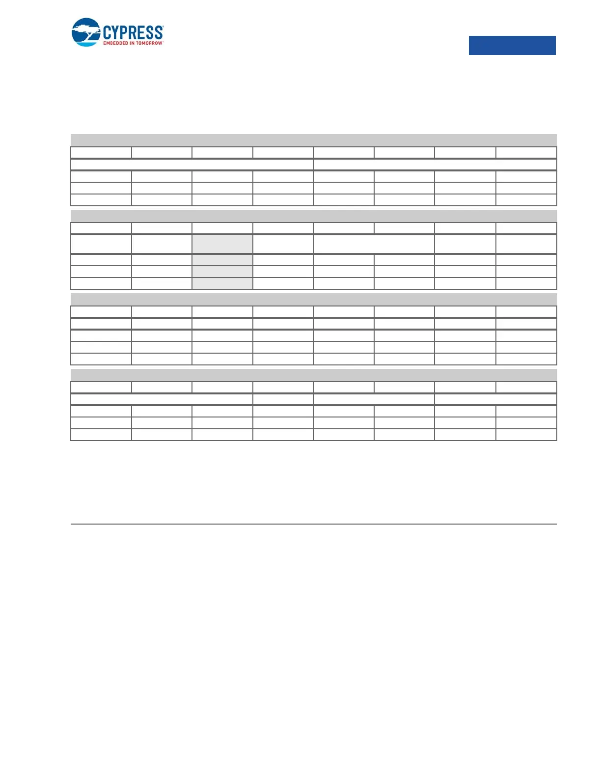
GPIF_BUS_CONFIG
0xE0014004
10.7.2 GPIF_BUS_CONFIG
Bus Configuration Register
This register specifies how the pins on the GPIF interface are distributed over data, address and control buses and which
special (hard-wired) functions are present on the control bus.
31:28 FIO1_CONF[3:0] Designates control to be used to enable output drivers of FIO1 (CTRL[8])
0 to 3 Use the alpha 4-7 to switch FIO1 direction.
8 to 11 Use beta 0-3.
27:24 FIO0_CONF[3:0] Designates control to be used to enable output drivers of FIO0 (CTRL[7])
0 to 3 Use the alpha 4 to 7 to switch FIO0 direction.
8 to 11 Use beta 0-3.
23 CE_CLKSTOP 0 Normal operation
1 CTRL[0] is CE; it should be used to clock gate most of GPIF when deasserted
22 INT_CTRL 0 Normal operation of INT pin
1 Override INT pin and connect to CTRL[15]
20 DRQ_ASSERT_MODE 0 Do nothing
1 Assert DRQ on rising edge of DMA_READY. Typical case, DRQ_MODE = 2, this bit 1.
continued on next page
GPIF_BUS_CONFIG Bus Configuration Register 0xE0014004
b31 b30 b29 b28 b27 b26 b25 b24
FIO1_CONF[3:0] FIO0_CONF[3:0]
R/W R/W R/W R/W R/W R/W R/W R/W
RRRRRRRR
00000000
GPIF_BUS_CONFIG Bus Configuration Register
b23 b22 b21 b20 b19 b18 b17 b16
CE_CLKSTOP INT_CTRL
DRQ_ASSERT_
MODE
DRQ_MODE[1:0] ALE_PRESENT CNTR_PRESENT
R/W R/W R/W R/W R/W R/W R/W
RR
RRRRR
00
00000
GPIF_BUS_CONFIG Bus Configuration Register
b15 b14 b13 b12 b11 b10 b9 b8
FIO1_PRESENT FIO0_PRESENT DRQ_PRESENT OE_PRESENT DLE_PRESENT WE_PRESENT CE_PRESENT ADR_CTRL[3]
R/W R/W R/W R/W R/W R/W R/W R/W
RRRRRRRR
00000000
GPIF_BUS_CONFIG Bus Configuration Register
b7 b6 b5 b4 b3 b2 b1 b0
ADR_CTRL[2:0] MUX_MODE BUS_WIDTH[1:0] PIN_COUNT[1:0]
R/W R/W R/W R/W R/W R/W R/W R/W
RRRRRRRR
00000000
Bit Name Description
 Loading...


