EZ-USB FX3 Technical Reference Manual, Document Number: 001-76074 Rev. *F 35
FX3 CPU Subsystem
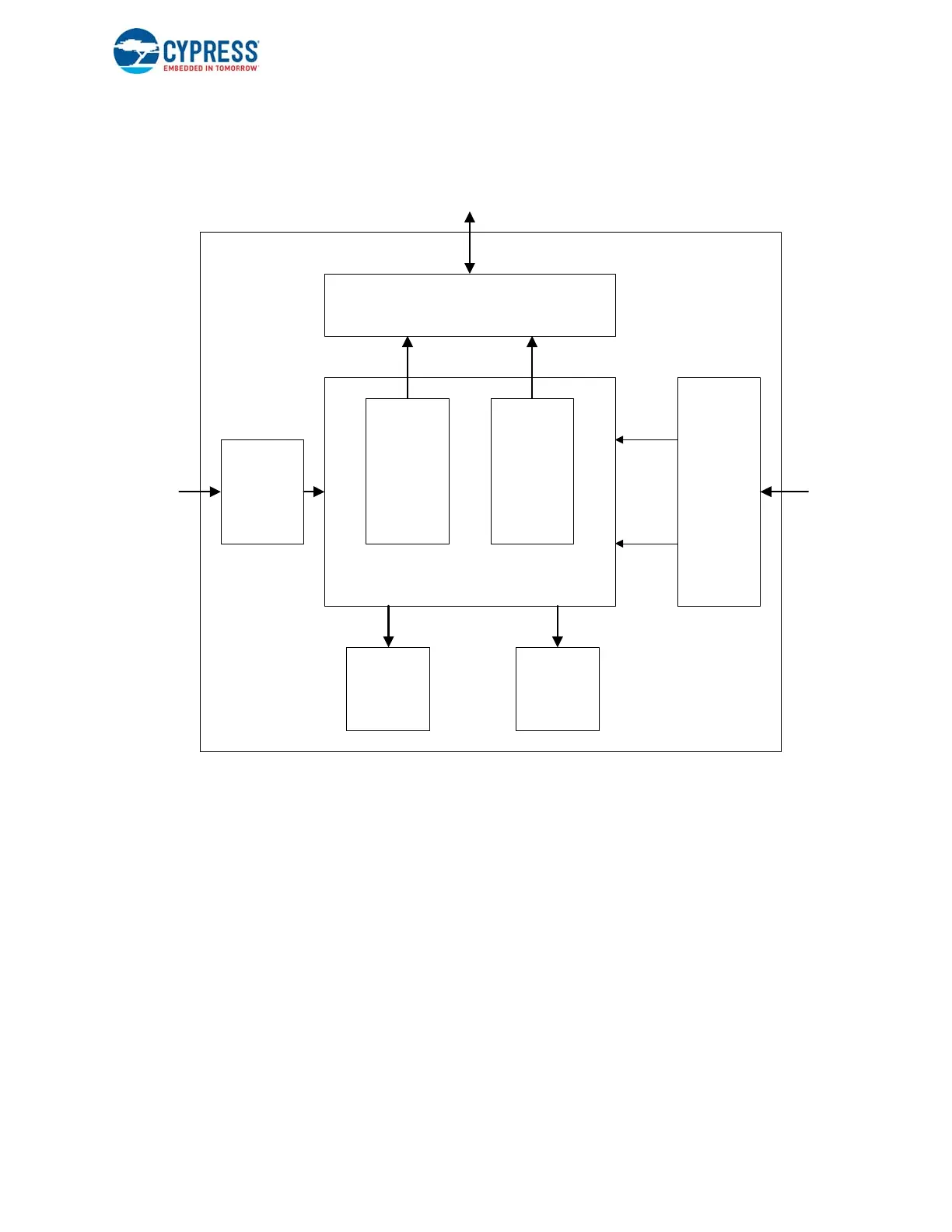
2.2 Block Diagram
Figure 2-1. CPU Subsystem in FX3 Device
2.3 Functional Overview
Figure 2-1 shows the ARM9 core and the associated blocks in the FX3 device. The CPU is associated with TCM blocks that
enable zero-latency accesses to performance-critical instructions and data, and it provides separate instruction and data
caches for other memory accesses. The PL192 VIC manages interrupts raised by the FX3 hardware blocks.
2.3.1 ARM926EJ-S CPU
The FX3 device has an embedded 32-bit ARM926EJ-S CPU core. This makes the device capable of implementing
multitasking applications where high performance and low power consumption are important.
This ARM9 core supports both 32-bit ARM instructions and 16-bit thumb instructions. The processor has separate advanced
high-performance bus (AHB) interfaces for internal instruction and data accesses. It also has separate instruction and data
TCM interfaces.
Note: The 32-bit ARM instruction set is commonly used in the FX3 SDK from Cypress, as this makes it more convenient to
address all of the available device memory.
Instruction
Cache
(8 KB)
Data
Cache
(8 KB)
ARM926EJ-S Core
AHB Bridge
Instruction AHB
(32 bit x 200 MHz)
Data AHB
(32 bit x 200 MHz)
FX3 System Interconnect (AHB)
PL192
VIC
nIRQ
nFIQ
Interrupt
Requests
ITCM
(16 KB)
DTCM
(8 KB)
Single Cycle ARM TCM Access
(32 bit x 200 MHz)
JTAG
TAP
JTAG
Interface

 Loading...


