EZ-USB FX3 Technical Reference Manual, Document Number: 001-76074 Rev. *F 258
GCTL_PLL_CFG
0xE0052000
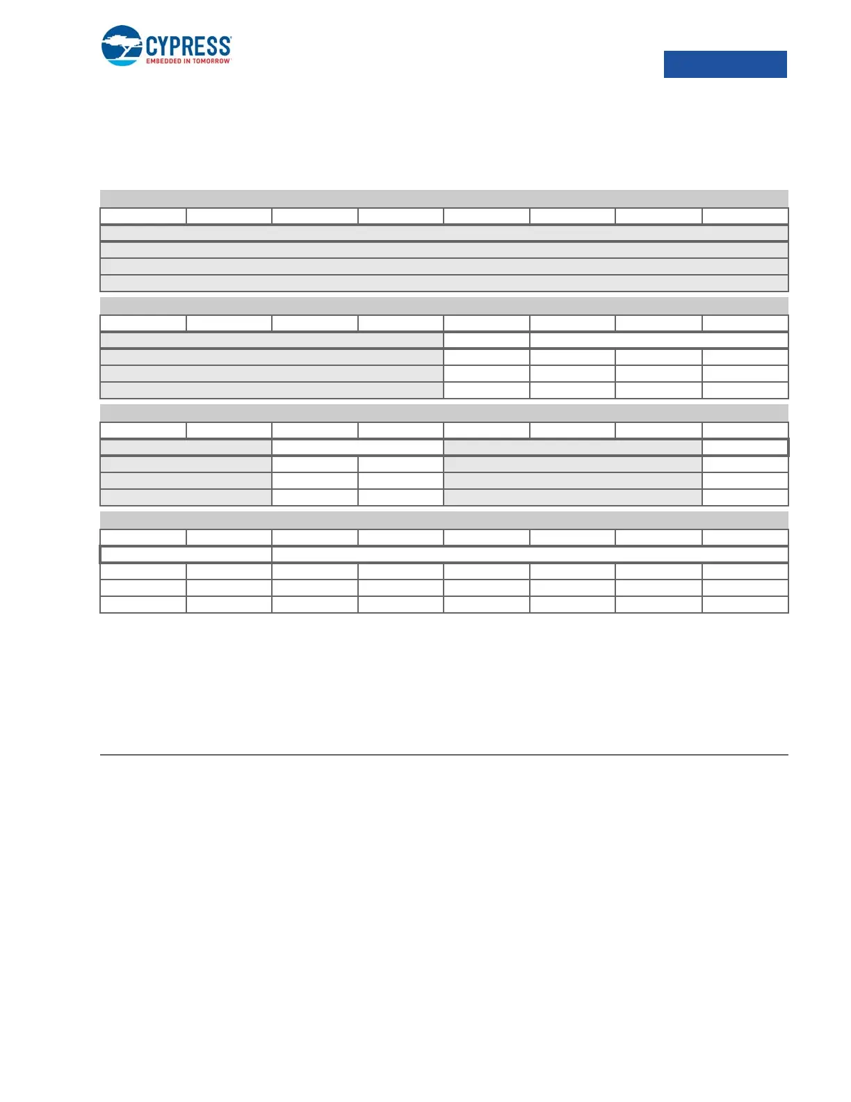
10.4.11 GCTL_PLL_CFG
PLL Configuration Register
On power up, this value is initialized depending on the FSLC[1:0] pin values as follows:
0: 19.2-MHz input clock, FBDIV = 20, REFDIV0 = 0, OUTDIV(1:0) = 00, oscclk = 384 MHz
FX3 supports only 19.2 MHz.
19 PLL_LOCK Asserted when PLL locks
18:16 FSLC Value presented on FSLC[2:0] pins on the device that identify reference clock frequency/crystal pro-
vided. FSLC[2] selects between reference clock or crystal, FSLC[1:0] select reference clock fre-
quency when FSLC[2] = 0.
13:12 CP_CFG PLL charge pump configuration
0 2.5 µA
15 µA
2 7.5 µA
3 10 µA
The charge pump bit setting varies depending on both the refclk frequency and the configuration
divider bits.
continued on next page
GCTL_PLL_CFG PLL Configuration Register 0xE0052000
b31 b30 b29 b28 b27 b26 b25 b24
GCTL_PLL_CFG PLL Configuration Register
b23 b22 b21 b20 b19 b18 b17 b16
PLL_LOCK FSLC[2:0]
RRRR
R/W R/W R/W R/W
0XXX
GCTL_PLL_CFG PLL Configuration Register
b15 b14 b13 b12 b11 b10 b9 b8
CP_CFG[1:0] REFDIV
R/W R/W R/W
RR R/W
00 H
GCTL_PLL_CFG PLL Configuration Register
b7 b6 b5 b4 b3 b2 b1 b0
OUTDIV[1:0] FBDIV[5:0]
R/W R/W R/W R/W R/W R/W R/W R/W
R R R/W R/W R/W R/W R/W R/W
0 0HHHHHH
Bit Name Description

 Loading...


