EZ-USB FX3 Technical Reference Manual, Document Number: 001-76074 Rev. *F 65
FX3 DMA Subsystem
5.5.4.4 ALIGNMENT REQUIREMENT - How Not To Share Cache Lines
The basic requirement is that DMA buffers that may be modified by the hardware should not share a cache line with software
data elements. This translates to a requirement that all DMA buffers which may be used for ingress (data coming in to FX3
and being written into memory by the DMA hardware) transfers should be 32-byte aligned and occupy an integral number of
cache lines (32 bytes each).
This restriction only applies to DMA buffers that may be used for ingress data transfers. The restriction does not apply to DMA
buffers that are used only as a source of egress data.
5.5.5 Sockets
A socket is the unidirectional virtual port (gateway) used by a peripheral (IP) block to transfer data to/ from the system SRAM.
Each DMA transfer involves one or two sockets. A socket represents either the consuming or the producing half of a transfer.
For a transfer from one peripheral to another, two sockets are involved. A socket is either a consuming socket or a producing
socket at any point in time-not both at the same time.
An FX3 DMA-capable peripheral has multiple sockets in the DMA adapter. The number of sockets and their properties
depend on the specific DMA adapter to the peripheral. Each peripheral block (IP block) in the device can support a predefined
number of sockets which is the maximum number of independent data flows that can be done through that IP at a given point
of time. A producer (ingress) socket is one which moves data from the IP block to the system SRAM. A consumer (egress)
socket is one which takes data from the system SRAM and moves it out through the IP block. Each socket can be identified
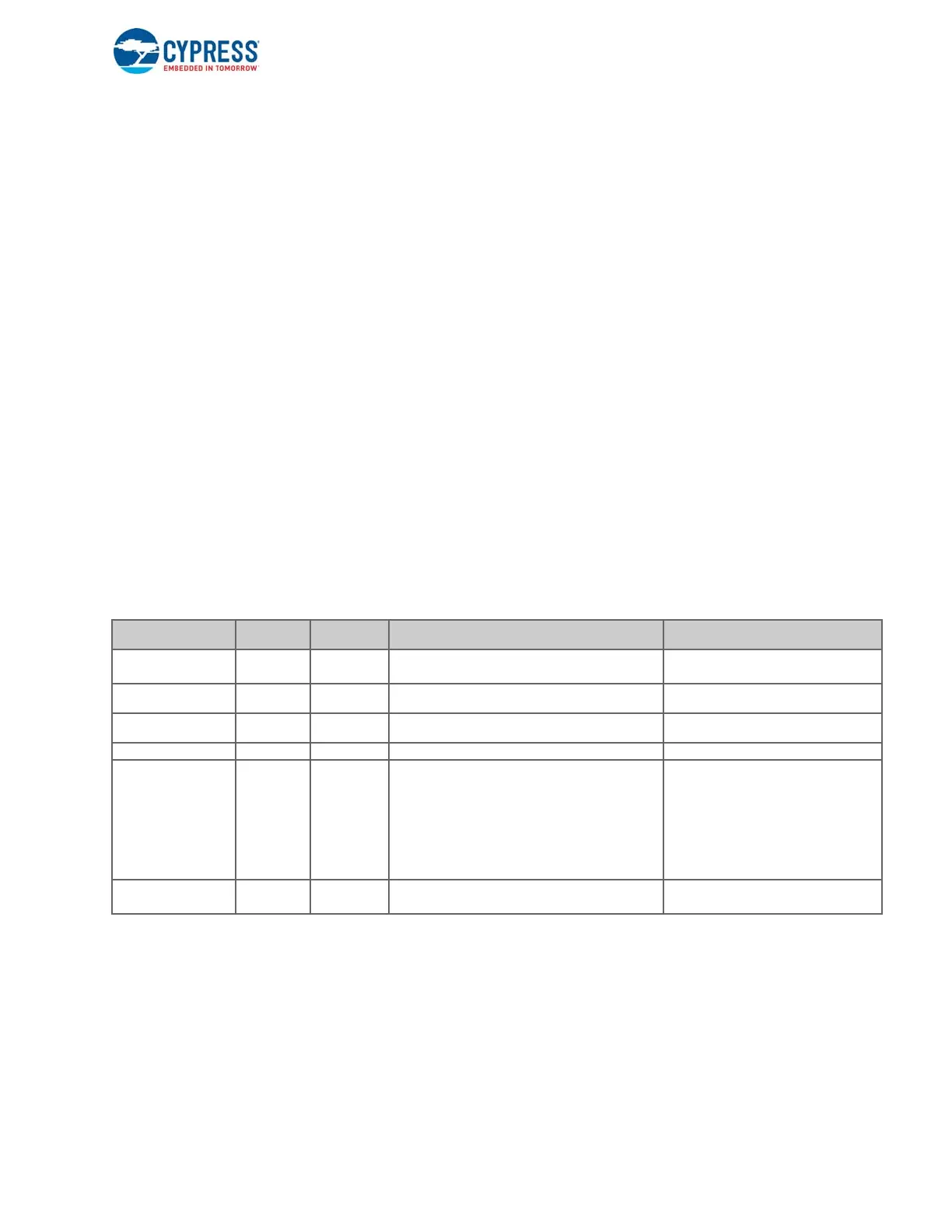
with the IP number and the socket number. Ta ble 5 - 2 is the socket summary for each FX3 peripheral.
Note: Separate DMA adapters are used for USB IN and OUT endpoints to allow greater USB data bandwidth. Interrupts from
both adapters are combined into a single interrupt vector.
Table 5-2. Peripheral DMA Sockets
Each socket has its own register set that the firmware uses to control the DMA operations. The socket register base address
is located at offset 0x8000 from the base address of the peripheral.
Each register set occupies a 128-byte address space with some gaps in between. Figure 5-7 details the socket registers and
their field definitions.
SCK_DSCR on page 605 describes the current descriptor to be loaded for this socket.
SCK_SIZE on page 607 sets the amount of data to be transferred. A zero value in this register means the data amount is
infinite.
FX3 Peripheral/
IP block
IP_NUM Socket Count Specific Property Notes
GPIF II 0x01 32
Socket 0-15: Bidirectional Socket
16-31: Ingress only
USB 0x03 16 Socket 0-15 for USB Egress: Egress Only
This maps to IN endpoints where FX3 sends
data out.
USB-IN 0x04 16 Socket 0-15 for USB Ingress: Ingress Only
This maps to OUT endpoints where FX3
receives data.
Storage 0x02 8 All are Bidirectional FX3S Only
Serial Peripherals
(UART, I2C, I2S, SPI)
0x00 8
Socket 0-1 for I2S: Egress only
Socket 2 for I2C data out: Egress only
Socket 3 for UART data out: Egress only
Socket 4 for SPI data out: Egress only
Socket 5 for I2C data in: Ingress only
Socket 6 for UART data in: Ingress only
Socket 7 for SPI data in: Ingress only
The purpose of each socket in this adapter
is fixed and cannot be changed.
CPU 0x3F 2
Socket 0 for CPU data in
Socket 1 for CPU data out

 Loading...


