EZ-USB FX3 Technical Reference Manual, Document Number: 001-76074 Rev. *F 260
GCTL_CPU_CLK_CFG
0xE0052004
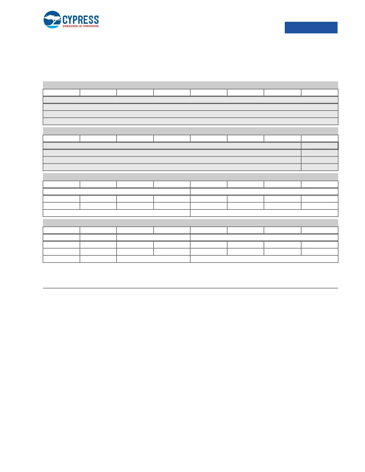
10.4.12 GCTL_CPU_CLK_CFG
CPU and Bus Clock Configuration Register
15:12 MMIO_DIV[3:0] MMIO bus clock divider value. This determines how much to divide the CPU clock. The actual divider
is DIV + 1. Zero (divide by 1) is illegal and results in undefined behavior. In other words, the range of
divider values is 2 to16. The following must be true: (MMIO_DIV + 1) = N × (DMA_DIV +1).
11:8 DMA_DIV[3:0] DMA bus clock divider value. This determines how much to divide the CPU clock. The actual divider
is DIV + 1. Zero (divide by 1) is illegal and results in undefined behavior. In other words, the range of
divider values is 2 to 16.
5:4 SRC[1:0] Clock source select. This field selects between one of the following four prestage system clocks
00 sys16_clk (sys_clk_pll divided by 16)
01 sys4_clk (sys_clk_pll divided by 4)
10 sys2_clk (sys_clk_pll divided by 2)
11 sys_clk_pll
On power up, the CPU clock will be PLL clock divided by 2, which is around 100 MHz. The expecta-
tion is that Boot ROM/Firmware changes this value to get to final CPU frequency.
3:0 CPU_DIV CPU clock divider value. This determines how much to divide the source clock selected by the SRC
field of this register. The actual divider is DIV + 1. Zero (divide by 1) is illegal and results in undefined
behavior. In other words, the range of divider values is 2 to 16.
GCTL_CPU_CLK_CFG CPU and Bus Clock Configuration Register 0xE0052004
b31 b30 b29 b28 b27 b26 b25 b24
GCTL_CPU_CLK_CFG CPU and Bus Clock Configuration Register
b23 b22 b21 b20 b19 b18 b17 b16
GCTL_CPU_CLK_CFG CPU and Bus Clock Configuration Register
b15 b14 b13 b12 b11 b10 b9 b8
MMID_DIV[3:0] DMA_DIV[11:8]
R/W R/W R/W R/W R/W R/W R/W R/W
RRRRRRRR
1
1
GCTL_CPU_CLK_CFG CPU and Bus Clock Configuration Register
b7 b6 b5 b4 b3 b2 b1 b0
00 SRC[1:0] CPU_DIV[3:0]
R R R/W R/W R/W R/W R/W R/W
RRRRRRRR
00
2 1
Bit Name Description
 Loading...


