EZ-USB FX3 Technical Reference Manual, Document Number: 001-76074 Rev. *F 465
SHDL_OHCI
0xE0032400
10.14.34 SHDL_OHCI (continued)
This area exposes the scheduler memory in OHCI format. Note that the EHCI and OHCI scheduler memories are using the
same physical memory, so overwriting one will also overwrite the other. Scheduler memory consists of three sections:
1. Lower Section:
2. Upper Section:
3. Scratch Section:
This register exposes only the Lower and Upper section. The Scratch section is only used by Hardware and it is not accessi-
ble by Software. The Lower and Upper sections each consist of 32 End Points and each End Point requires 3 32-bit scheduler
memory locations. In result, the MMIO address for lower section would be x400-x57C and for upper portion would be x580-
x6FC. Software can update the appropriate portion of the memory based on the PERI_SHDL_STATUS/ASYNC_SHDL_STA-
TUS bits in the UIB_HOST_SHDL_CS register.
continued on next page
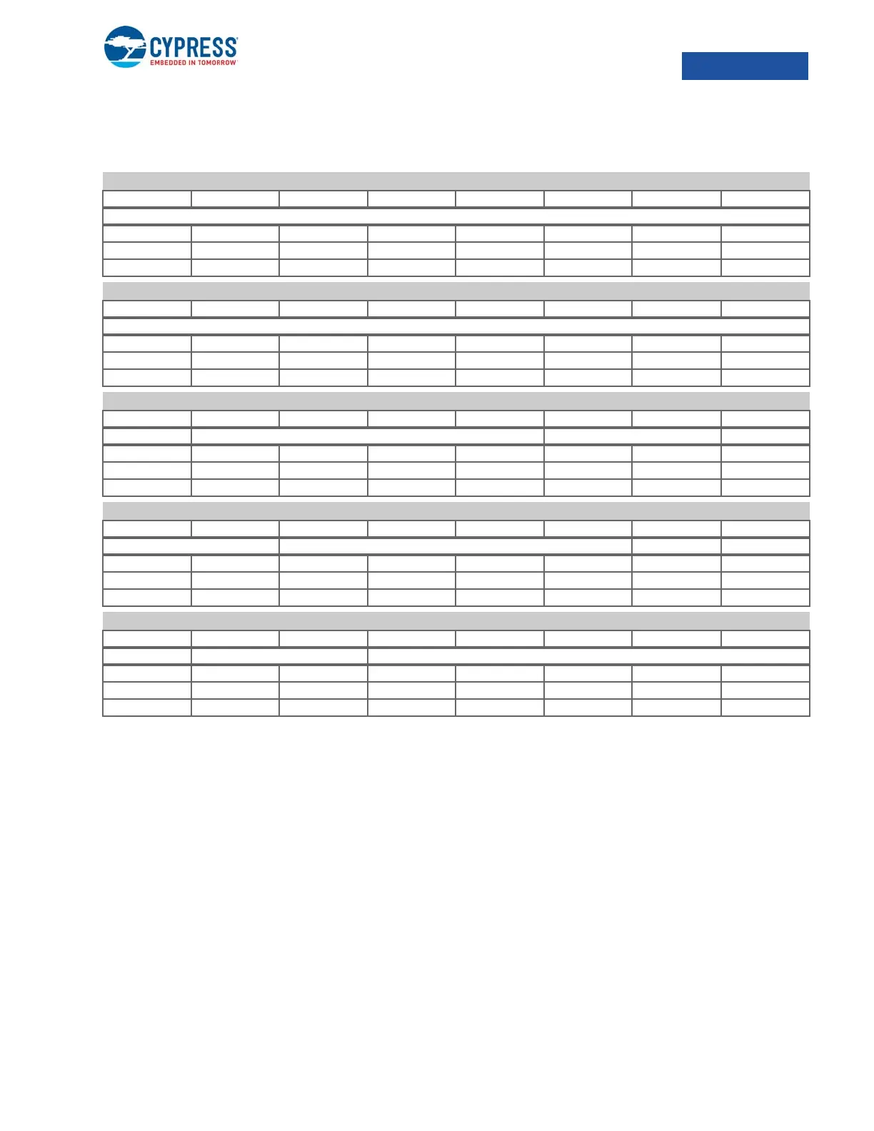
SHDL_OHCI Scheduler Memory Register, OHCI Format
b39 b38 b37 b36 b35 b34 b33 b32
MAX_PKT_SIZE[7:0]
R/W R/W R/W R/W R/W R/W R/W R/W
RRRRRRRR
00000000
SHDL_OHCI Scheduler Memory Register, OHCI Format
b31 b30 b29 b28 b27 b26 b25 b24
UFRAME_SMASK[7:0]
R/W R/W R/W R/W R/W R/W R/W R/W
RRRRRRRR
00000000
SHDL_OHCI Scheduler Memory Register, OHCI Format
b23 b22 b21 b20 b19 b18 b17 b16
PING RL[3:0] MULT[1:0] ISO_EPM
R/W R/W R/W R/W R/W R/W R/W R/W
RRRRRRRR
00000000
SHDL_OHCI Scheduler Memory Register, OHCI Format
b15 b14 b13 b12 b11 b10 b9 b8
CERR[1:0] NAK_CNT[3:0] HALT T
R/W R/W R/W R/W R/W R/W R/W R/W
RRRRRRRR
00000000
SHDL_OHCI Scheduler Memory Register, OHCI Format
b7 b6 b5 b4 b3 b2 b1 b0
ZPLEN EPT[1:0] EPND[4:0]
R/W R/W R/W R/W R/W R/W R/W R/W
RRRRRRRR
00000000

 Loading...


