EZ-USB FX3 Technical Reference Manual, Document Number: 001-76074 Rev. *F 55
Global Controller (GCTL)
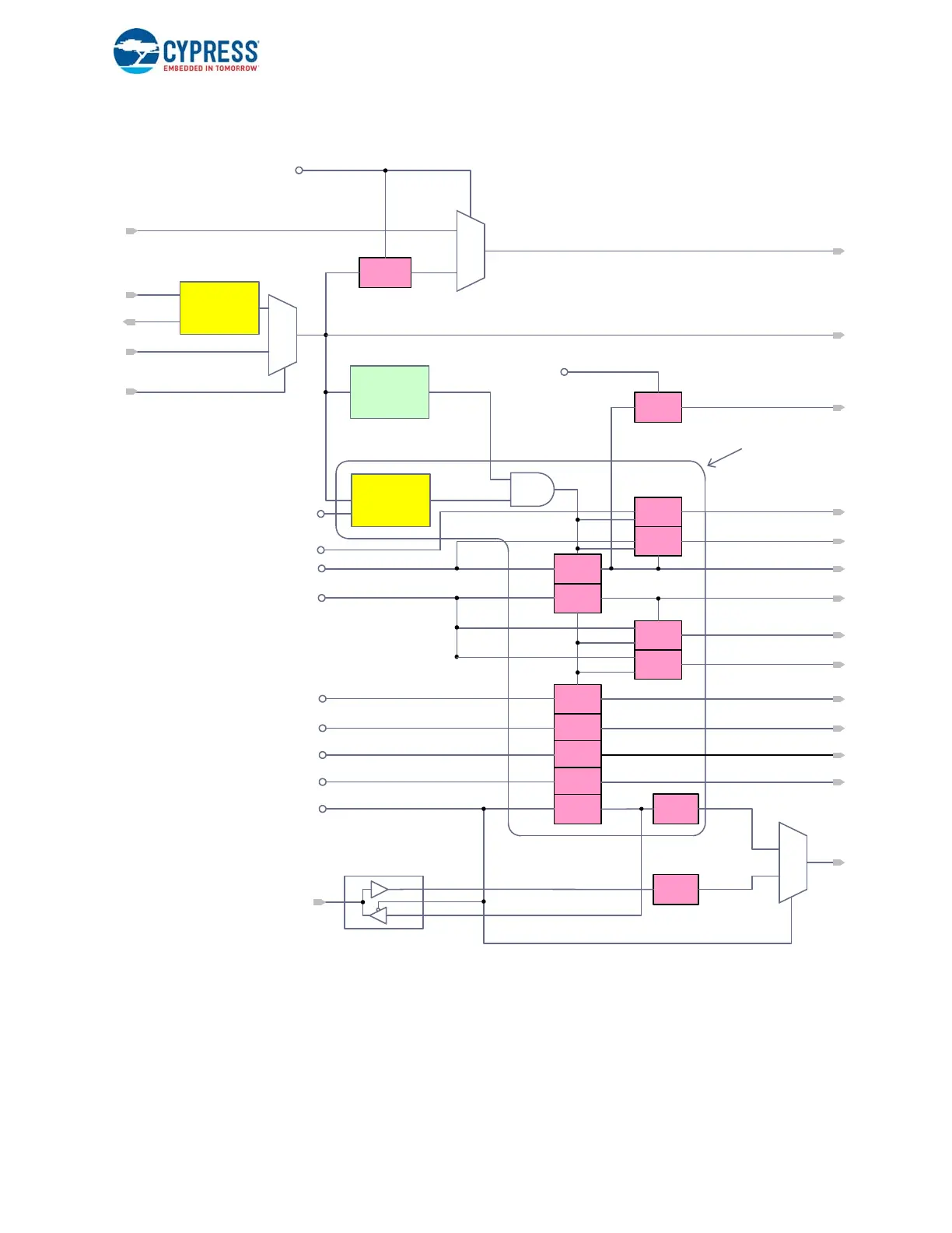
Figure 4-1. Clock System Block Diagram
Four system clocks are obtained by dividing the master clock by 1, 2, 4, and 16. The system clocks are then used to generate
clocks for most peripherals in the device through the respective Clock Select and Divide (CSD) block. A CSD block is used to
select one of the four system clocks and then divide it using the specified divider value. The depth of the divider is different for
different peripherals.
The CPU clock is derived by selecting and dividing one of the four system clocks by an integer factor between 1 and 16. The
bus clocks are derived from the CPU clock. Independent 4-bit dividers are provided for both the DMA and MMIO bus clocks.
The frequency of the MMIO clock, however, must be an integer divide of the DMA clock frequency. It is not recommended to
50us
Delay
CSD
/4
XTAL
Osc
CSD
CSD
CSD
CSD
CSD
CSD
CSD
CSD
CSD
CSD
CSD
PLL
/4
CSD
GCTLBACKUP
CLKIN_32
XTALIN
XTALOUT
CLKIN
FSLC[2]
GCTL_PLL_CFG
GCTL_GPIO_SLOW_CLK_CFG
GCTL_GPIO_FAST_CLK_CFG
GCTL_CPU_CLK_CFG
GCTL_PIB_CLK_CFG
GCTL_I2C_CLK_CFG
GCTL_UART_CLK_CFG
GCTL_SPI_CLK_CFG
GCTL_I2S_CLK_CFG
StandbyClock
ReferenceClock
StandbyEdge
StandbyGPIOClock
SlowGPIOClock
SimpleGPIOClock
FastGPIOClock
CPUClock
DMAClock
MMIOClock
PIBClock
I2CClock
UARTClock
SPIClock
I2SClock
pad
in
out
oe_n
enable
enable
Master(System)Clock
GCTL

 Loading...


