Home
Cypress
Controller
EZ-USB FX3
Cypress EZ-USB FX3 User Manual
4
of 1
of 1 rating
660 pages
Give review
Manual
Specs
To Next Page
To Next Page
To Previous Page
To Previous Page
Loading...
EZ-USB FX3 T
echnical R
eference Manual, Documen
t Number: 001-760
74 Rev
. *F
160
General Programmable Interface I
I (GPIF II)
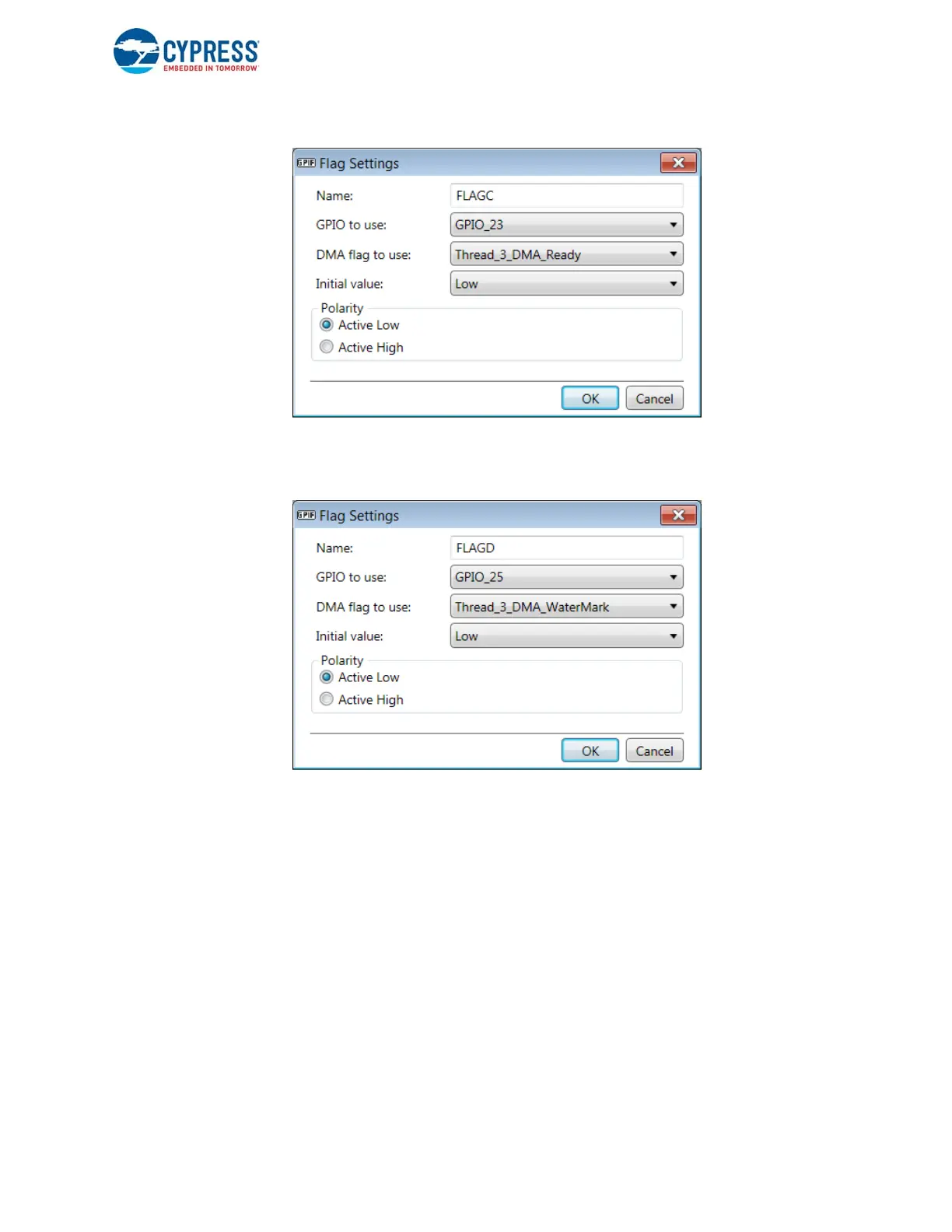
Figure 7-48. FL
AGC Settings
Figure
7-49
shows
the FLAGD settings.
Figure 7-49. FL
AGD Settings
A
screen shot
of the Interf
ace Definition window
with the previ
ous settings is
shown in
Figure
7-50
.
159
161
Table of Contents
Default Chapter
3
Table of Contents
3
1 Introduction to EZ-USB FX3
19
Overview of USB 3.0
19
Physical Layer
19
Link Layer
20
Protocol Layer
21
Unicast Transactions
21
Token/ Data/Handshake Sequences
21
Data Bursting
23
End-To-End Flow Control
24
Streams
25
Superspeed Power Management
25
Function Power Management
26
FX3/FX3S Features
26
FX3 Block Diagram
28
FX3S Block Diagram
29
Functional Overview
29
Cpu
29
Dma
30
USB Interface
30
Gpif II
30
UART Interface
31
I2C Interface
31
I2S Interface
31
SPI Interface
31
JTAG Interface
31
Storage Interface
31
SD/MMC Clock Stop
32
SD_CLK Output Clock Stop
32
Card Insertion and Removal Detection
32
Write Protection (WP)
32
SDIO Interrupt
32
SDIO Read-Wait Feature
32
Boot Options
32
Clocking
33
2 FX3 CPU Subsystem
34
Features
34
Block Diagram
35
Functional Overview
35
Arm926Ej-S Cpu
35
Processor Modes
36
Processor Registers
37
Exception Vectors
38
Mmu
38
Cache Memories
39
Tightly Coupled Memories
39
JTAG Interface
40
Vectored Interrupt Controller
40
CPU Operating Frequency
42
CPU Power Modes
42
Timers
43
3 Memory and System Interconnect
44
Features
44
Block Diagram
44
Functional Overview
45
Memory Regions
45
System Interconnect
47
Low-Power Operations
47
Cache Operations
48
Cache Coherency
48
Memory Usage
49
4 Global Controller (GCTL)
51
GPIO Pins
51
I/O Matrix Configuration
51
I/O Drive Strength
53
GPIO Pull-Up and Pull-Down
53
Simple GPIO Override
53
Complex GPIO Override
53
I/O Power Observability
54
Gctl_Iopower
54
Gctl_Iopwr_Intr
54
Gctl_Iopwr_Intr_Mask
54
Clock Management
54
Power Management
56
Power Domains
56
Power Modes
57
Reset
57
Hard Reset
57
Soft Reset
57
5 FX3 DMA Subsystem
58
DMA Introduction
58
DMA Features
58
DMA Block Diagram
58
DMA Overview
59
DMA Subsystem Components
60
Clocking
60
Descriptors Buffers, and Sockets
61
DMA Descriptors
61
DMA Buffer
63
Implications of Data Cache Usage
63
Memory Corruption Due to Cache Line Overlap
64
Safe Usage of Data Cache
64
Sockets
65
ALIGNMENT REQUIREMENT - How Not to Share Cache Lines
65
Software Manipulation of Sockets
68
Initializing a Socket
68
Terminating a Socket
68
Modifying or Suspending a Socket
68
Inspecting a Socket
69
Wrapping up a Socket
69
Illustration of Descriptor, Buffer and Socket Usage
69
Understanding DMA Operation: Peripheral to Peripheral
69
Interrupt Requests
71
DMA Interrupts
71
Programming Sequence
72
Initialization
72
Producer Half
72
Consumer Half
72
Peripheral to Peripheral Transfer
73
CPU Intervention in between Ingress and Egress
76
Concept of DMA Channels
77
6 Universal Serial Bus (USB)
78
Introduction
78
Features
78
Block Diagram
78
Overview
79
USB Interface Block
79
USB 3.0 Function Controller
79
USB 2.0 Function Controller
79
USB 2.0 Embedded Host
79
USB OTG Controller
80
End-Point Memory
80
DMA Adapters
80
USB I/O System
80
Usb 2.0 Otg Phy
80
Usb 3.0 Phy
81
UIB Top-Level Register Interface
81
USB Function Controllers
83
USB 3.0 Function
83
Clocking
83
Interrupt Requests
83
USB 3.0 Functional Description
84
Physical Layer
85
Link Layer
86
Protocol Layer
87
USB 2.0 Function
89
Clocking
89
Interrupt Requests
89
USB 2.0 Functional Description
89
Serial Interface Engine
89
Token Processor
89
USB 2.0 Function Registers
90
USB Reset
90
USB Suspend
90
USB Resume
90
Start of Frame
90
SETUP Packet
90
IN Packet
91
OUT Packet
91
USB 3.0 and USB 2.0 Function Coordination
91
USB Function Programming Model
92
USB 3.0 Initialization
92
USB 3.0 Enable
93
USB 3.0 Fallback to USB 2.0
94
USB Reset
95
USB Connect
96
USB Disconnect
98
Control Request
99
USB Embedded Host
106
Clocking
106
Interrupt Requests
106
Functional Description
107
Embedded Host
107
Scheduler Memory
107
Embedded Host Programming Model
109
Host Connect
109
Host Disconnect
109
Managing Transfers
110
USB OTG Controller
112
Interrupt Requests
112
USB OTG Programming Model
112
USB OTG Start and Stop
112
Session Request Protocol
116
Host Negotiation Protocol
118
7 General Programmable Interface II (GPIF II)
120
Features
120
Block Diagram
121
Typical GPIF II Interface
121
Functional Overview
122
Actions
122
Action - IN_DATA
124
Action - IN_ADDR
125
Action - DR_DATA
125
Action - DR_ADDR
126
Action - COMMIT
127
Action - DR_GPIO
127
Action - LD_ADDR_COUNT
128
Action - LD_DATA_COUNT
128
Action - LD_CTRL_COUNT
129
Action - COUNT_ADDR
130
Action - COUNT_DATA
130
Action - COUNT_CTRL
130
Action - CMP_ADDR
130
Action - CMP_DATA
131
Action - CMP_CTRL
131
Action - INTR_CPU
132
Action - INTR_HOST
132
Action - DR_DRQ
132
Triggers
133
Transition Conditions
133
GPIF II Designer Tool
134
GPIF II Hardware Resources
134
Comparators
134
Counters
135
GPIF II Interrupt
135
Threads and Sockets
135
Difference between PP_MODE=0 and PP_MODE=1
135
Addressing
137
Number of Address Lines
137
Assigning Sockets to Threads
137
Addressing Methods
137
Async/Sync
138
Configuration of Flags
138
Developing the GPIF II State Machine
138
Designing a GPIF II Interface
138
GPIF II State Machine Implementation
141
Add a State
141
Add Actions to a State
142
Draw Transitions between Actions
142
Add a Transition Equation
143
Set State Properties
143
Analyzing the Signal Timing of the GPIF II Interface
144
Selection of Time Frame
144
Automatic Timing Scale Selection
144
Scenario Entry
144
Macro
146
GPIF II Constraints
146
Mirror States
146
Mirror State Rules
147
Mirror State Example
148
Guidelines for Transition Equation Entry
149
Intermediate States
150
Initialization and Configuration of GPIF II Block
151
GPIF II State Machine Control
151
Performing Read and Write Operations Using GPIF II
151
DMA Channel Creation in FX3 Firmware to Perform GPIF II to USB Data Transfers
153
GPIF II State Machine to Read Data into a Socket
153
DMA Channel Creation in FX3 Firmware to Perform USB to GPIF II Data Transfers
154
GPIF II State Machine to Drive Data from Socket as Data Source
155
Alpha Values
156
GPIF II Read and Write over Registers
156
Implementing Synchronous Slave FIFO Interface
158
Synchronous Slave FIFO Access Sequence and Interface Timing
161
Synchronous Slave FIFO Read Sequence Description
162
Synchronous Slave FIFO Write Sequence Description
164
Slave FIFO Interface Logical Diagram
165
GPIF II State Machine of Slave FIFO Interface
165
8 Low Performance Peripherals (LPP)
167
I2C Interface
168
I2C Block Features
168
I2C Interface Overview
169
FX3 I2C Operations Overview
170
Reset and Initialization
170
Preamble
170
Data Transfer
170
Programming Model
170
Register-Based I2C Transfers
171
DMA-Based I2C Transfers
171
Starting a Transaction
171
Terminating Transactions: Software and Hardware Aborts
172
Multimaster Arbitration
172
Error Conditions
172
Examples
172
Initialize I2C Block
172
Configure I2C Block
173
Reads and Writes Using Register Transfers
173
Reads and Writes Using DMA Transfers
174
Serial Peripheral Interface
175
SPI Block Features
175
SPI Interface Overview
176
FX3 SPI Operations Overview
177
Reset and Initialization
177
Modes Governing Transfers
177
SSN Control Configurations
177
Data Transfers
178
Programming Model
178
Register-Based Transfers
178
DMA-Based Transfers
178
Examples
179
Initialize SPI Block
179
Configure SPI Block
179
Reads and Writes Using Register Transfers
180
Reads and Writes Using DMA Transfers
181
Universal Asynchronous Receiver Transmitter
183
UART Block Features
183
UART Overview
183
FX3 UART Operations Overview
184
Reset and Initialization
184
Programming Model
184
Register-Based Transfers
184
DMA-Based Transfers
184
Error Conditions
185
Examples
185
Initialize UART Block
185
Send UART Messages and Receive Fixed Bytes of Text
185
Integrated Interchip Sound Interface
187
I2S Block Features
187
I2S Overview
187
FX3 I2S Operations Overview
188
Programming Model
188
Start Transmission
188
Mute Condition
188
Pause Condition
188
Buffer Underflow
189
Stop Event
189
Fixed Clock Mode
189
Data Shift Mode
189
Padding
189
Error Conditions
189
Examples
189
Initialize I2S Block
190
Configure I2S Interface
190
Transfer Data from USB to I2S Interface Using DMA Transfers
190
Gpio
192
GPIO Features
192
GPIO Overview
192
Programming Model
192
Reset and Initialization
192
Examples
193
Initialize GPIO Block
193
Configure GPIO[45] as Input Pin and GPIO[21] as Output Pin
194
Configure GPIO[50] to Generate PWM Output
196
9 Storage Ports
197
Storage Interface Block Features
197
Block Diagram
197
Storage Interface (S-Port)
199
SD/ MMC/ SDIO Interface
201
SD/MMC Interface Overview
201
SDIO Interface Overview
203
FX3S S-Port Operations Overview
203
S-Port Initialization and Configuration
204
Configuring the FX3S I/O Matrix
204
Setting S-Port Interface Parameters
204
Starting the Storage Driver
205
Setting the S-Port Clock
206
Sending SD/MMC/SDIO Commands
206
Handling SIB Events
208
Reads and Writes to SD/ MMC Using DMA Transfers
210
Sending Vendor Commands to SD/ MMC
212
Setting the Granularity of Write Operations
212
Checking Card Status
212
Aborting Ongoing Transaction to S-Port
212
Working with SDIO Cards
213
Configuration and Initialization
213
Reads and Writes from SDIO Card Registers
213
IO_RW_DIRECT Command (CMD52)
213
Setting Function Block Size
218
Initialization and Operation of SDIO Functions
218
SDIO Interrupts
218
Enabling and Disabling SDIO Interrupts
219
Handling SDIO Interrupts
219
FX3S-Specific Features
220
Card Insertion and Removal Detection Mechanism
220
Handling Card Detection in Software
221
Write Protection
222
Sd/MMC Clock Stop
222
SD_CLK Output Clock Stop
222
SDIO Read-Wait/ Suspend-Resume Feature
222
Read-Wait
222
Suspend-Resume Feature
223
SD3.0 Host Tuning Feature
223
Normal and Alternate Emmc4.4 Boot
224
10 Registers
228
Introduction
228
Register Conventions
229
Vectored Interrupt Controller (VIC) Registers
230
Vic_Irq_Status
230
Vic_Fiq_Status
231
Vic_Raw_Status
232
Vic_Int_Select
233
Vic_Int_Enable
234
Vic_Int_Clear
235
Vic_Priority_Mask
236
Vic_Vec_Address
237
Vic_Vect_Priority
238
Vic_Address
239
Global Controller Registers
240
Gctl_Iomatrix
240
Gctl_Gpio_Simple
241
Gctl_Gpio_Complex
243
Gctl_Ds
245
Gctl_Wpu_Cfg
247
Gctl_Wpd_Cfg
249
Gctl_Iopower
251
Gctl_Iopower_Intr
253
Gctl_Iopower_Intr_Mask
255
Gctl_Sw_Int
257
Gctl_Pll_Cfg
258
Gctl_Cpu_Clk_Cfg
260
Gctl_Uib_Core_Clk
261
Gctl_Pib_Core_Clk
262
Gctl_Gpio_Fast_Clk
263
Gctl_Gpio_Slow_Clk
265
Gctl_I2C_Core_Clk
266
Gctl_Uart_Core_Clk
267
Gctl_Spi_Core_Clk
268
Gctl_I2S_Core_Clk
269
Global Controller Always on Registers
270
Gctl_Wakeup_En
270
Gctl_Wakeup_Polarity
272
Gctl_Wakeup_Event
274
Gctl_Freeze
276
Gctl_Watchdog_Cs
277
Gctl_Watchdog_Timer0
279
Gctl_Watchdog_Timer1
280
PIB Registers
281
Pib_Config
281
Pib_Intr
283
Pib_Intr_Mask
285
Pib_Clock_Detect
287
Pib_Rd_Mailbox
288
Pib_Wr_Mailbox
290
Pib_Error
292
Pib_Eop_Eot
294
Pib_Dll_Ctrl
295
Pib_Wr_Threshold
297
Pib_Rd_Threshold
298
Pib_Id
299
Pib_Power
300
GPIF Registers
301
Gpif_Config
301
Gpif_Bus_Config
303
Gpif_Bus_Config2
305
Gpif_Ad_Config
306
Gpif_Status
308
Gpif_Intr
310
Gpif_Intr_Mask
312
Gpif_Ctrl_Bus_Direction
314
Gpif_Ctrl_Bus_Default
315
Gpif_Ctrl_Bus_Polarity
316
Gpif_Ctrl_Bus_Toggle
317
Gpif_Ctrl_Bus_Select
318
Gpif_Ctrl_Count_Config
319
Gpif_Ctrl_Count_Reset
320
Gpif_Ctrl_Count_Limit
321
Gpif_Addr_Count_Config
322
Gpif_Addr_Count_Reset
323
Gpif_Addr_Count_Limit
324
Gpif_State_Count_Config
325
Gpif_State_Count_Limit
326
Gpif_Data_Count_Config
327
Gpif_Data_Count_Reset
328
Gpif_Data_Count_Limit
329
Gpif_Ctrl_Comp_Value
330
Gpif_Ctrl_Comp_Mask
331
Gpif_Data_Comp_Value
332
Gpif_Data_Comp_Mask
333
Gpif_Addr_Comp_Value
334
Gpif_Addr_Comp_Mask
335
Gpif_Data_Ctrl
336
Gpif_Ingress_Data
337
Gpif_Egress_Data
338
Gpif_Ingress_Address
339
Gpif_Egress_Address
340
Gpif_Thread_Config
341
Gpif_Lambda_Stat
343
Gpif_Alpha_Stat
344
Gpif_Beta_Stat
345
Gpif_Waveform_Ctrl_Stat
346
Gpif_Waveform_Switch
348
Gpif_Waveform_Switch_Timeout
350
Gpif_Beta_Deassert
351
Gpif_Function
352
Gpif_Left_Waveform
353
Gpif_Right_Waveform
356
P-Port Registers
359
Pp_Id
359
Pp_Init
360
Pp_Config
361
Pp_Intr_Mask
363
Pp_Drqr5_Mask
364
Pp_Sock_Mask
365
Pp_Error
366
Pp_Dma_Xfer
367
Pp_Dma_Size
368
Pp_Wr_Mailbox
369
Pp_Mmio_Addr
371
Pp_Mmio_Data
372
Pp_Mmio
373
Pp_Event
374
Pp_Rd_Mailbox
376
Pp_Sock_Stat
378
Pp_Buf_Size_Cnt
379
USB Port Registers
380
Uib_Intr
380
Uib_Intr_Mask
382
Uib_Id
384
Uib_Power
385
USB2 HS/FS/LS PHY Registers
386
Phy_Clk_And_Test
386
Phy_Conf
388
Phy_Chirp
390
USB2 Device Controller Registers
391
Dev_Cs
391
Dev_Framecnt
393
Dev_Pwr_Cs
394
Dev_Setupdat
395
Dev_Toggle
397
Dev_Epi_Cs
399
Dev_Epi_Xfer_Cnt
401
Dev_Epo_Cs
402
Dev_Epo_Xfer_Cnt
404
Dev_Ctrl_Intr_Mask
405
Dev_Ctrl_Intr
406
Dev_Ep_Intr_Mask
407
Dev_Ep_Intr
408
USB Controller Miscellaneous Registers
409
Chgdet_Ctrl
409
Chgdet_Intr
411
Chgdet_Intr_Mask
412
Otg_Ctrl
413
Otg_Intr
415
Otg_Intr_Mask
416
Otg_Timer
417
USB End Point Manager Registers
418
Eepm_Cs
418
Iepm_Cs
420
Iepm_Mult
421
Eepm_Endpoint
422
Iepm_Endpoint
423
Iepm_Fifo
424
USB2 Host Controller Registers
425
Host_Cs
425
Host_Ep_Intr
426
Host_Ep_Intr_Mask
427
Host_Toggle
428
Host_Shdl_Cs
430
Host_Shdl_Sleep
432
Host_Resp_Base
433
Host_Resp_Cs
434
Host_Active_Ep
435
Ohci_Revision
436
Ohci_Control
437
Ohci_Command_Status
438
Ohci_Interrupt_Status
439
Ohci_Interrupt_Enable
440
Ohci_Interrupt_Disable
441
Ohci_Fm_Interval
442
Ohci_Fm_Remaining
443
Ohci_Fm_Number
444
Ohci_Periodic_Start
445
Ohci_Ls_Threshold
446
Ohci_Rh_Port_Status
447
Ohci_Eof
449
Ehci_Hccparams
450
Ehci_Usbcmd
451
Ehci_Usbsts
452
Ehci_Usbintr
453
Ehci_Frindex
454
Ehci_Configflag
455
Ehci_Portsc
456
Ehci_Eof
458
Shdl_Chng_Type
459
Shdl_State_Machine
460
Shdl_Internal_Status
462
Shdl_Ohci
464
Shdl_Ehci
468
USB3 Link Controller Registers
472
Lnk_Conf
472
Lnk_Intr
473
Lnk_Intr_Mask
475
Lnk_Error_Conf
477
Lnk_Error_Status
479
Lnk_Error_Count
481
Lnk_Error_Count_Threshold
482
Lnk_Phy_Conf
483
Lnk_Phy_Mpll_Status
484
Lnk_Phy_Tx_Trim
485
Lnk_Phy_Error_Conf
486
Lnk_Phy_Error_Status
487
Lnk_Device_Power_Control
489
Lnk_Ltssm_State
491
Lnk_Lfps_Observe
492
Lnk_Compliance_Pattern_0
493
Lnk_Compliance_Pattern_1
494
Lnk_Compliance_Pattern_2
495
Lnk_Compliance_Pattern_3
496
Lnk_Compliance_Pattern_4
497
Lnk_Compliance_Pattern_5
498
Lnk_Compliance_Pattern_6
499
Lnk_Compliance_Pattern_7
500
Lnk_Compliance_Pattern_8
501
USB3 Protocol Layer Registers
502
Prot_Cs
502
Prot_Intr
504
Prot_Intr_Mask
506
Prot_Framecnt
508
Prot_Itp_Time
509
Prot_Itp_Timestamp
510
Prot_Setup_Dat
511
Prot_Seq_Num
513
Prot_Ep_Intr
515
Prot_Ep_Intr_Mask
516
Prot_Epi_Cs1
517
Prot_Epi_Cs2
519
Prot_Epi_Unmapped_Stream
520
Prot_Epi_Mapped_Stream
521
Prot_Epo_Cs1
522
Prot_Epo_Cs2
524
Prot_Epo_Unmapped_Stream
525
Prot_Epo_Mapped_Stream
526
USB Port - Superspeed Ingress Socket Registers
527
Uibin_Id
527
Uibin_Power
528
I2S Registers
529
I2S_Config
529
I2S_Status
531
I2S_Intr
533
I2S_Intr_Mask
534
I2S_Egress_Data_Left
535
I2S_Egress_Data_Right
536
I2S_Counter
537
I2S_Socket
538
I2S_Id
539
I2S_Power
540
I2C Registers
541
I2C_Config
541
I2C_Status
543
I2C_Intr
545
I2C_Intr_Mask
546
I2C_Timeout
547
I2C_Dma_Timeout
548
I2C_Preamble_Ctrl
549
I2C_Preamble_Data
550
I2C_Preamble_Rpt
552
I2C_Command
553
I2C_Egress_Data
555
I2C_Ingress_Data
556
I2C_Clock_Low_Count
557
I2C_Byte_Count
558
I2C_Bytes_Transferred
559
I2C_Socket
560
I2C_Id
561
I2C_Power
562
UART Registers
563
Uart_Config
563
Uart_Status
565
Uart_Intr
567
Uart_Intr_Mask
568
Uart_Egress_Data
569
Uart_Ingress_Data
570
Uart_Socket
571
Uart_Rx_Byte_Count
572
Uart_Tx_Byte_Count
573
Uart_Id
574
Uart_Power
575
SPI Registers
576
Spi_Config
576
Spi_Status
578
Spi_Intr
580
Spi_Intr_Mask
581
Spi_Egress_Data
582
Spi_Ingress_Data
583
Spi_Socket
584
Spi_Rx_Byte_Count
585
Spi_Tx_Byte_Count
586
Spi_Id
587
Spi_Power
588
General Purpose IO Block Registers
589
Gpio_Simple
589
Gpio_Invalue0
591
Gpio_Invalue1
592
Gpio_Intr0
593
Gpio_Intr1
594
Gpio_Intr
595
Gpio_Id
596
Gpio_Power
597
General Purpose IO Registers (One Pin)
598
Pin_Status
598
Pin_Timer
600
Pin_Period
601
Pin_Threshold
602
Low Performance Peripherals Registers
603
Lpp_Id
603
Lpp_Power
604
DMA Socket and Descriptor Registers
605
Sck_Dscr
605
Sck_Size
607
Sck_Count
608
Sck_Status
609
Sck_Intr
612
Sck_Intr_Mask
614
Dscr_Buffer
616
Dscr_Sync
617
Dscr_Chain
619
Dscr_Size
620
Event
622
DMA Adapter Global Registers
623
Sck_Intr
623
Adapter_Status
629
Sib_Id
630
Sib_Power
631
Sdmmc_Cmd_Idx
632
Sdmmc_Cmd_Arg0
633
Sdmmc_Cmd_Arg1
634
Sdmmc_Resp_Idx
635
Sdmmc_Resp_Reg0
636
Sdmmc_Resp_Reg1
637
Sdmmc_Resp_Reg2
638
Sdmmc_Resp_Reg3
639
Sdmmc_Resp_Reg4
640
Sdmmc_Cmd_Resp_Fmt
641
Sdmmc_Block_Count
642
Sdmmc_Block_Len
643
Sdmmc_Mode_Cfg
644
Sdmmc_Data_Cfg
646
Sdmmc_Cs
647
Sdmmc_Status
649
Sdmmc_Intr
651
Sdmmc_Intr_Mask
653
Sdmmc_Ncr
655
Sdmmc_Ncc_Nwr
656
Sdmmc_Nac
657
Sdmmc_Hw_Ctrl
658
4
Based on 1 rating
Ask a question
Give review
Questions and Answers:
Need help?
Do you have a question about the Cypress EZ-USB FX3 and is the answer not in the manual?
Ask a question
Cypress EZ-USB FX3 Specifications
General
Brand
Cypress
Model
EZ-USB FX3
Category
Controller
Language
English
Related product manuals
Cypress EZ-USB FX2LP
42 pages
Cypress EZ-USB CX3
35 pages
CapSense Express CY8CMBR3108
167 pages
Cypress EZ-USB FX3 SDK
56 pages
Cypress CY7C68013
48 pages

 Loading...


