317
────────────────────────────────────────────────────
14.4 SCSI Interface
────────────────────────────────────────────────────
1
2
3
4
5
21
7
8
9
10
11
12
13
14
A
14.4.1 SCSI Interface Specifications
Input signals
Receiver
Input signal levels
Maximum load current
Minimum hysteresis
CMOS receiver with hysteresis
Low level: 0 to 0.8 VDC, High level: 2.0 to 5.25 VDC
±
10
μ
A
(excluding terminator)
0.2 VDC
Output signals
Driver
Output signal levels
Driver sink current
Open-drain CMOS driver
Low level: 0 to 0.8 VDC, High level: 2.0 to 5.25 VDC
48 mA
Terminator power signal
Output voltage
Maximum output current
4to5.25VDC
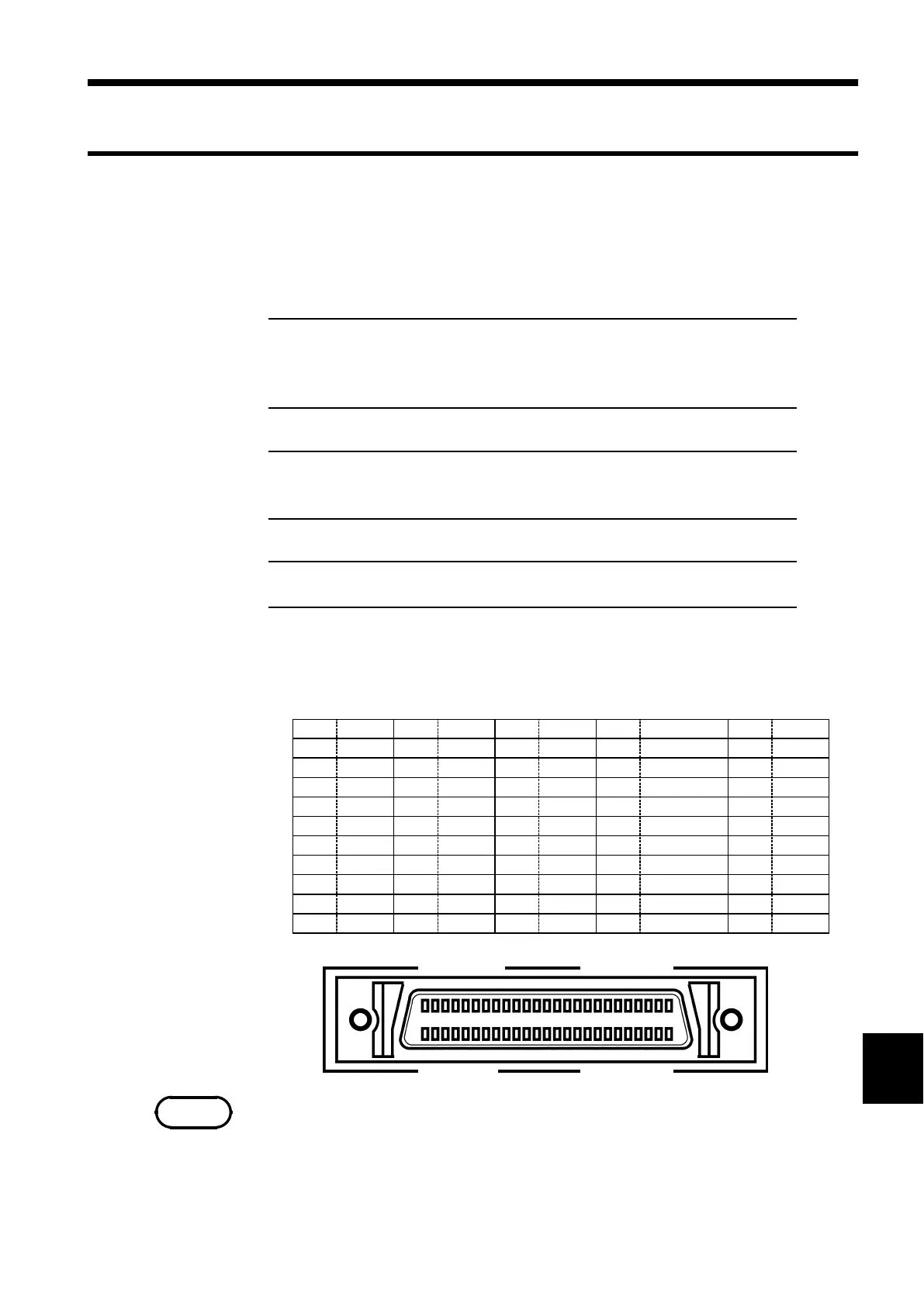
1.2 A
Pin Signal Pin Signal Pin Signal Pin Signal Pin Signal
1 GND 11 GND 21 GND 31 -DB5 41 -ATN
2 GND 12 GND 22 GND 32 -DB6 42 GND
3 GND 13 GND 23 GND 33 -DB7 43 -BSY
4 GND 14 GND 24 GND 34 -DBP 44 -ACK
5 GND 15 GND 25 GND 35 GND 45 -RST
6 GND 16 GND 26 -DB0 36 GND 46 -MSG
7 GND 17 GND 27 -DB1 37 GND 47 -SEL
8 GND 18 GND 28 -DB2 38 TERMPWR 48 -C/D
9 GND 19 GND 29 -DB3 39 GND 49 -REQ
10 GND 20 GND 30 -DB4 40 GND 50 -I/O
NOTE
14.4 SCSI Interface
■ General specifications
See Section 18.2.
■ Electrical specifications
■ Connector
Recommended connector:
Socket used: High density(pin type)(D-Sub half-pitch 50 P)
SCSI connector pin outs
・ The SCSI cable is not supplied.
・ Check the connection types on both the 8841/8842 and the connected
device. Use commercially-available SCSI cables.