RM0090 USB on-the-go full-speed (OTG_FS)
Doc ID 018909 Rev 4 1024/1422
30.3 OTG_FS functional description
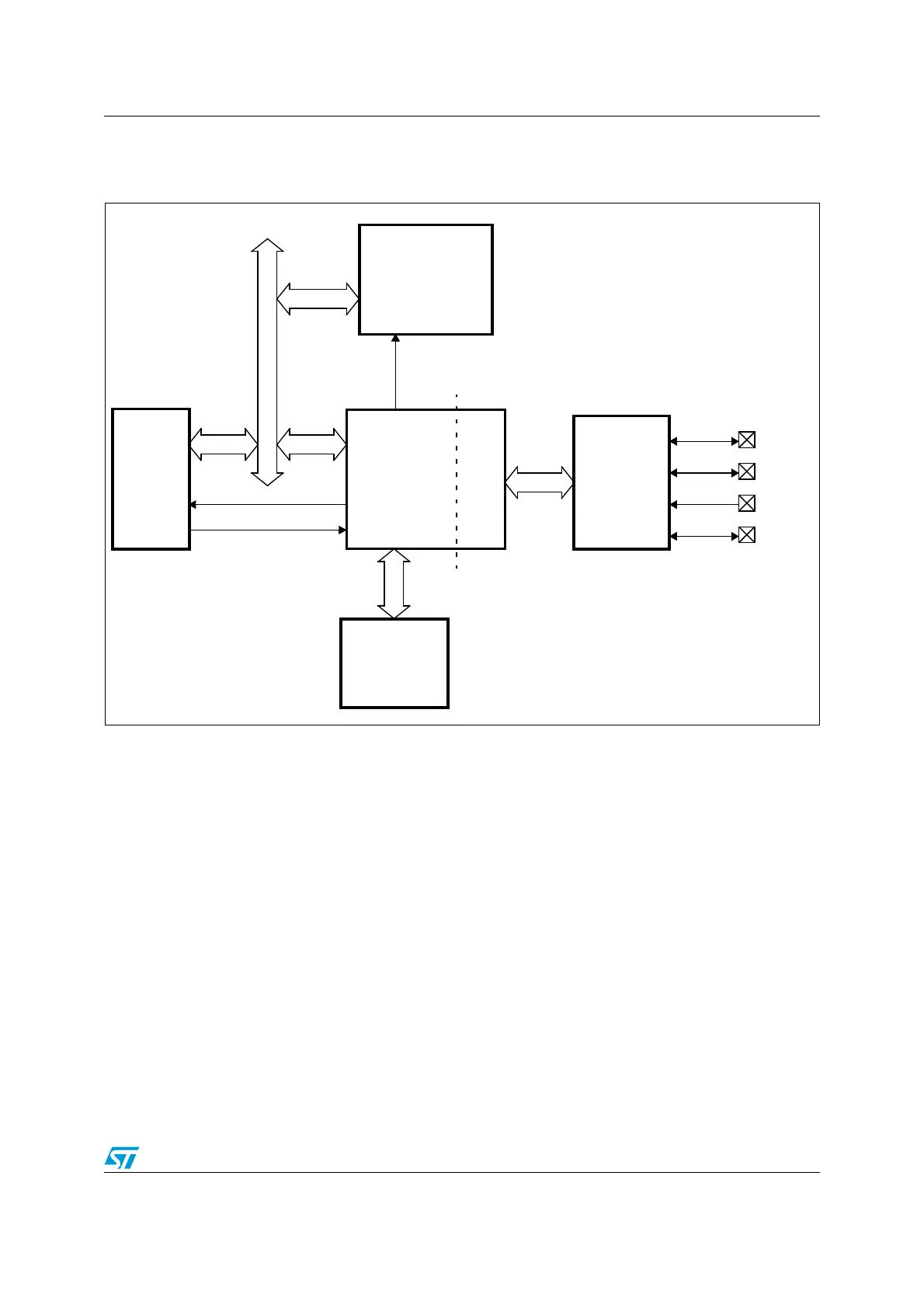
Figure 357. Block diagram
30.3.1 OTG full-speed core
The USB OTG FS receives the 48 MHz ±0.25% clock from the reset and clock controller
(RCC), via an external quartz. The USB clock is used for driving the 48 MHz domain at full-
speed (12 Mbit/s) and must be enabled prior to configuring the OTG FS core.
The CPU reads and writes from/to the OTG FS core registers through the AHB peripheral
bus. It is informed of USB events through the single USB OTG interrupt line described in
Section 30.15: OTG_FS interrupts.
The CPU submits data over the USB by writing 32-bit words to dedicated OTG_FS locations
(push registers). The data are then automatically stored into Tx-data FIFOs configured
within the USB data RAM. There is one Tx-FIFO push register for each in-endpoint
(peripheral mode) or out-channel (host mode).
The CPU receives the data from the USB by reading 32-bit words from dedicated OTG_FS
addresses (pop registers). The data are then automatically retrieved from a shared Rx-FIFO
configured within the 1.25 KB USB data RAM. There is one Rx-FIFO pop register for each
out-endpoint or in-channel.
The USB protocol layer is driven by the serial interface engine (SIE) and serialized over the
USB by the full-/low-speed transceiver module within the on-chip physical layer (PHY).
DP
DM
ID
V
BUS
OTG
FS
PHY
USB2.0
OTG FS
Core
UTMIFS
1.25 Kbytes
USB data
FIFOs
AHB Peripheral
Power&
Clock
CTRL
USB Interrupt
USB duspend
USB Clock at 48 MHz
Cortex-M4F
System clock
domain
USB clock
domain
Universal serial bus
RAM bus
MS19928V1

 Loading...


