RM0090 Cryptographic processor (CRYP)
Doc ID 018909 Rev 4 568/1422
before they are written into the OUT FIFO. For example, the operation would be byte
swapping for an ASCII text stream.
The kind of data to be processed is configured with the DATATYPE bitfield in the CRYP
control register (CRYP_CR).
Figure 214 shows how the 64-bit data block M1...64 is constructed from two consecutive 32-
bit words popped off the IN FIFO by the CRYP processor, according to the DATATYPE
value. The same schematic can easily be extended to form the 128-bit block for the AES
cryptographic algorithm (for the AES, the block length is four 32-bit words, but swapping only
takes place at word level, so it is identical to the one described here for the TDES).
Note: The same swapping is performed between the IN FIFO and the CRYP data block, and
between the CRYP data block and the OUT FIFO.
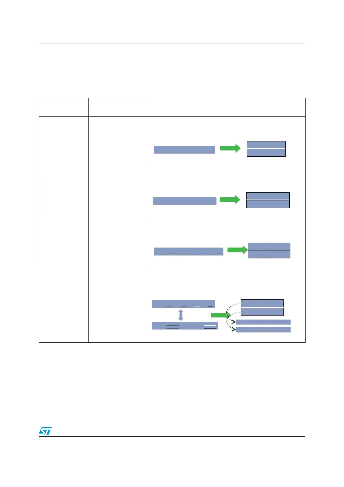
Table 91. Data types
DATATYPE in
CRYP_CR
Swapping performed
System memory data
(plaintext or cypher)
00b No swapping
Example: TDES block value 0xABCD77206973FE01 is
represented in system memory as:
01b
Half-word (16-bit)
swapping
Example: TDES block value 0xABCD77206973FE01 is
represented in system memory as:
10b Byte (8-bit) swapping
Example: TDES block value 0xABCD77206973FE01 is
represented in system memory as:
11b Bit swapping
TDES block value 0x4E6F772069732074 is represented in system
memory as:
0xABCD7720 6973FE01
TDES block size = 64bit = 2x 32 bit
0xABCD7720
0x6973FE01
@
@+4
system memory
0xABCD 7720 6973 FE01
TDES block size = 64bit = 2x 32 bit
0x7720 ABCD
0xFE01 6973
@
@+4
system memory
0xAB CD 77 20 69 73 FE 01
TDES block size = 64bit = 2x 32 bit
0x 20 77 CD AB
0x 01 FE 73 69
@
@+4
system memory
0x4E 6F 77 20 69 73 20 74
0x04 EE F6 72
0x2E 04 CE 96
@
@+4
0000 0100 1110 111 0 1111 0110 0111 0010
0100 1110 0110 1111 0111 011 1 0010 0000
0110 1001 0111 0011
0010 0000 0111 0100
0010 1110 0000 0100 1100 111 0 1001 0110
@
@+4
system memory
TDES Bloc size = 64bit = 2x 32 bit

 Loading...


