RM0090 Flexible static memory controller (FSMC)
Doc ID 018909 Rev 4 1320/1422
memory. Clearly, the device cannot be accessed in byte mode (only 16-bit words
can be read from/written to the Flash memory) therefore:
a) Write transactions are not allowed
b) Read transactions are allowed. All memory bytes are read and the useless ones
are discarded. The NBL[1:0] are set to 0 during read transactions.
Configuration registers
The FSMC can be configured using a register set. See Section 32.5.6, for a detailed
description of the NOR Flash/PSRAM control registers. See Section 32.6.8, for a detailed
description of the NAND Flash/PC Card registers.
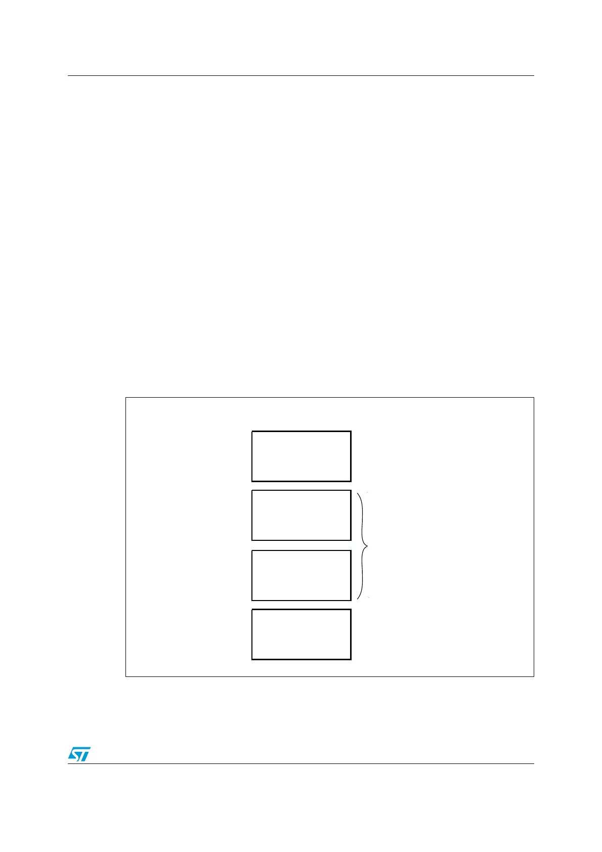
32.4 External device address mapping
From the FSMC point of view, the external memory is divided into 4 fixed-size banks of
256 Mbytes each (Refer to Figure 404):
● Bank 1 used to address up to 4 NOR Flash or PSRAM memory devices. This bank is
split into 4 NOR/PSRAM regions with 4 dedicated Chip Select.
● Banks 2 and 3 used to address NAND Flash devices (1 device per bank)
● Bank 4 used to address a PC Card device
For each bank the type of memory to be used is user-defined in the Configuration register.
Figure 404. FSMC memory banks
32.4.1 NOR/PSRAM address mapping
HADDR[27:26] bits are used to select one of the four memory banks as shown in Ta b l e 1 85 .
Bank 1
NAND Flash
NOR / PSRAM
Supported memory typeBanks
4 × 64 MB
6000 0000h
6FF F FFF Fh
Address
7000 0000h
7FF F FFF Fh
8000 0000h
8FF F FFF Fh
9000 0000h
9FF F FFF Fh
Bank 2
4 × 64 MB
Bank 3
4 × 64 MB
Bank 4
4 × 64 MB
PC Card
ai14719

 Loading...


