General-purpose timers (TIM9 to TIM14) RM0090
523/1422 Doc ID 018909 Rev 4
16.6.9 TIM10/11/13/14 capture/compare register 1 (TIMx_CCR1)
Address offset: 0x34
Reset value: 0x0000
16.6.10 TIM11 option register 1 (TIM11_OR)
Address offset: 0x50
Reset value: 0x0000
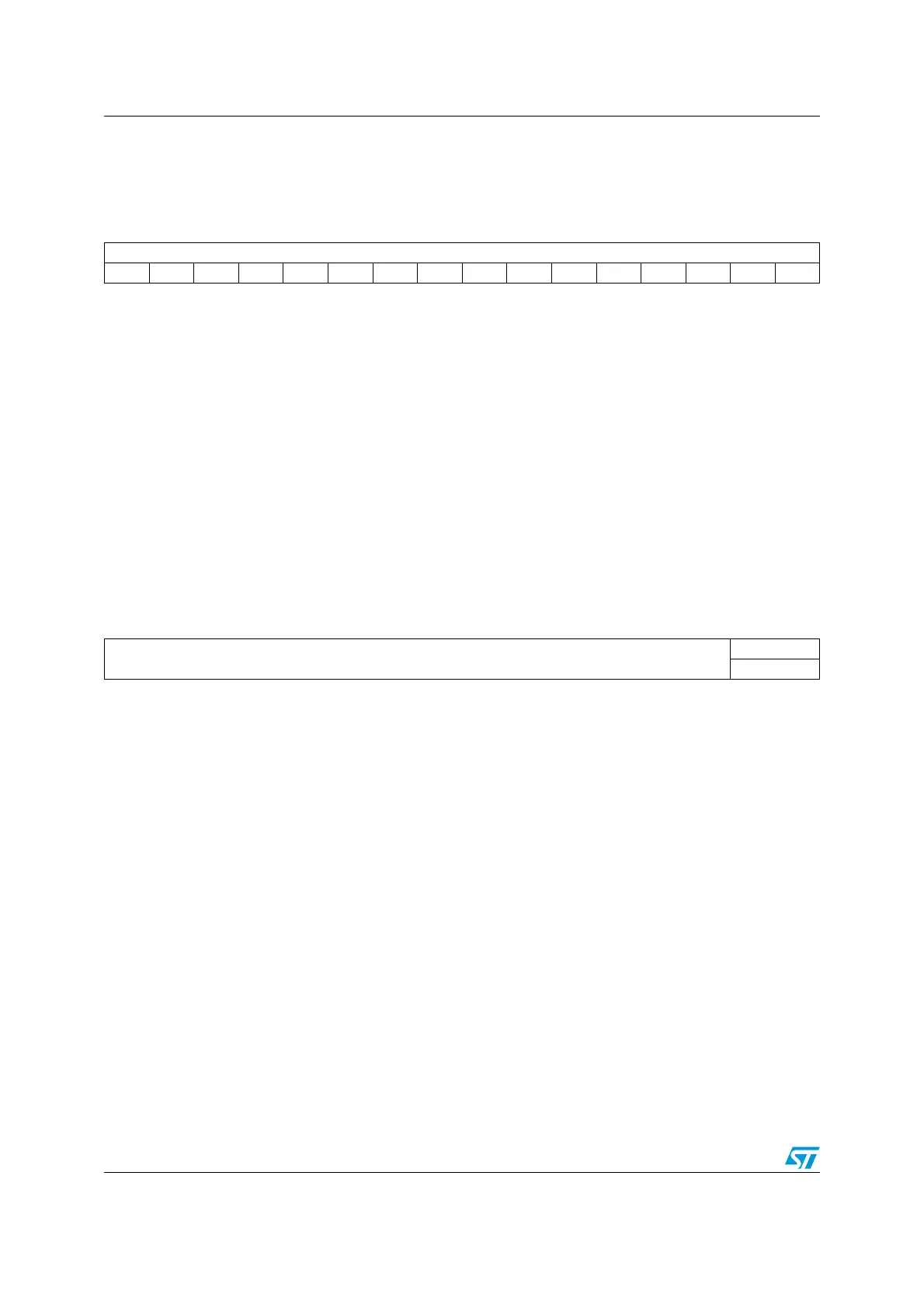
1514131211109876543210
CCR1[15:0]
rw rw rw rw rw rw rw rw rw rw rw rw rw rw rw rw
Bits 15:0 CCR1[15:0]: Capture/Compare 1 value
If channel CC1 is configured as output:
CCR1 is the value to be loaded in the actual capture/compare 1 register (preload value).
It is loaded permanently if the preload feature is not selected in the TIMx_CCMR1 register (bit
OC1PE). Else the preload value is copied in the active capture/compare 1 register when an
update event occurs.
The active capture/compare register contains the value to be compared to the counter
TIMx_CNT and signaled on OC1 output.
If channel CC1is configured as input:
CCR1 is the counter value transferred by the last input capture 1 event (IC1).
1514131211109876543210
Reserved
TI1_RMP[1:0]
rw
Bits 15:2 Reserved, must be kept at reset value.
Bits 1:0 TI1_RMP[1:0]: TIM11 Input 1 remapping capability
Set and cleared by software.
00,01,11: TIM11 Channel1 is connected to the GPIO (refer to the Alternate function
mapping table in the datasheets).
10: HSE_RTC clock (HSE divided by programmable prescaler) is connected to the
TIM11_CH1 input for measurement purposes

 Loading...


