RM0090 Embedded Flash memory interface
Doc ID 018909 Rev 4 82/1422
3.8.7 Flash option control register (FLASH_OPTCR)
The FLASH_OPTCR register is used to modify the user option bytes.
Address offset: 0x14
Reset value: 0x0FFF AAED. The option bits are loaded with values from Flash memory at
reset release.
Access: no wait state when no Flash memory operation is ongoing, word, half-word and
byte access.
Bit 2 MER: Mass Erase of bank 1 sectors
Erase activated of bank 1 sectors.
Bit 1 SER: Sector Erase
Sector Erase activated.
Bit 0 PG: Programming
Flash programming activated.
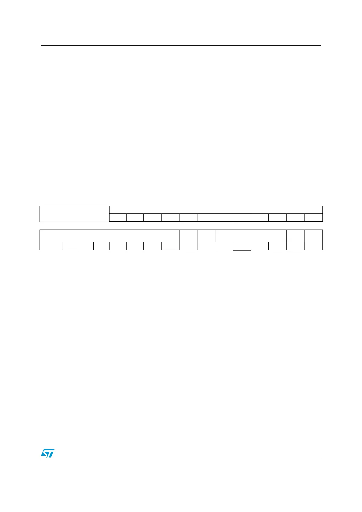
31 30 29 28 27 26 25 24 23 22 21 20 19 18 17 16
Reserved
nWRP[11:0]
rw rw rw rw rw rw rw rw rw rw rw rw
1514131211109876543210
RDP[7:0]
nRST_
STDBY
nRST_
STOP
WDG_
SW
Reserv
ed
BOR_LEV
OPTST
RT
OPTLO
CK
rw rw rw rw rw rw rw rw rw rw rw rw rw rs rs
Bits 31:28 Reserved, must be kept cleared.
Bits 27:16 nWRP: Not write protect
These bits contain the value of the write-protection option bytes of sectors after reset. They
can be written to program a new write protect value into Flash memory.
0: Write protection active on selected sector
1: Write protection not active on selected sector
Bits 15:8 RDP: Read protect
These bits contain the value of the read-protection option level after reset. They can be
written to program a new read protection value into Flash memory.
0xAA: Level 0, read protection not active
0xCC: Level 2, chip read protection active
Others: Level 1, read protection of memories active
Bits 7:5 USER: User option bytes
These bits contain the value of the user option byte after reset. They can be written to
program a new user option byte value into Flash memory.
Bit 7: nRST_STDBY
Bit 6: nRST_STOP
Bit 5: WDG_SW
Note: When changing the WDG mode from hardware to software or from software to
hardware, a system reset is required to make the change effective.
Bit 4 Reserved, must be kept cleared.

 Loading...


