RM0090 General-purpose I/Os (GPIO)
Doc ID 018909 Rev 4 196/1422
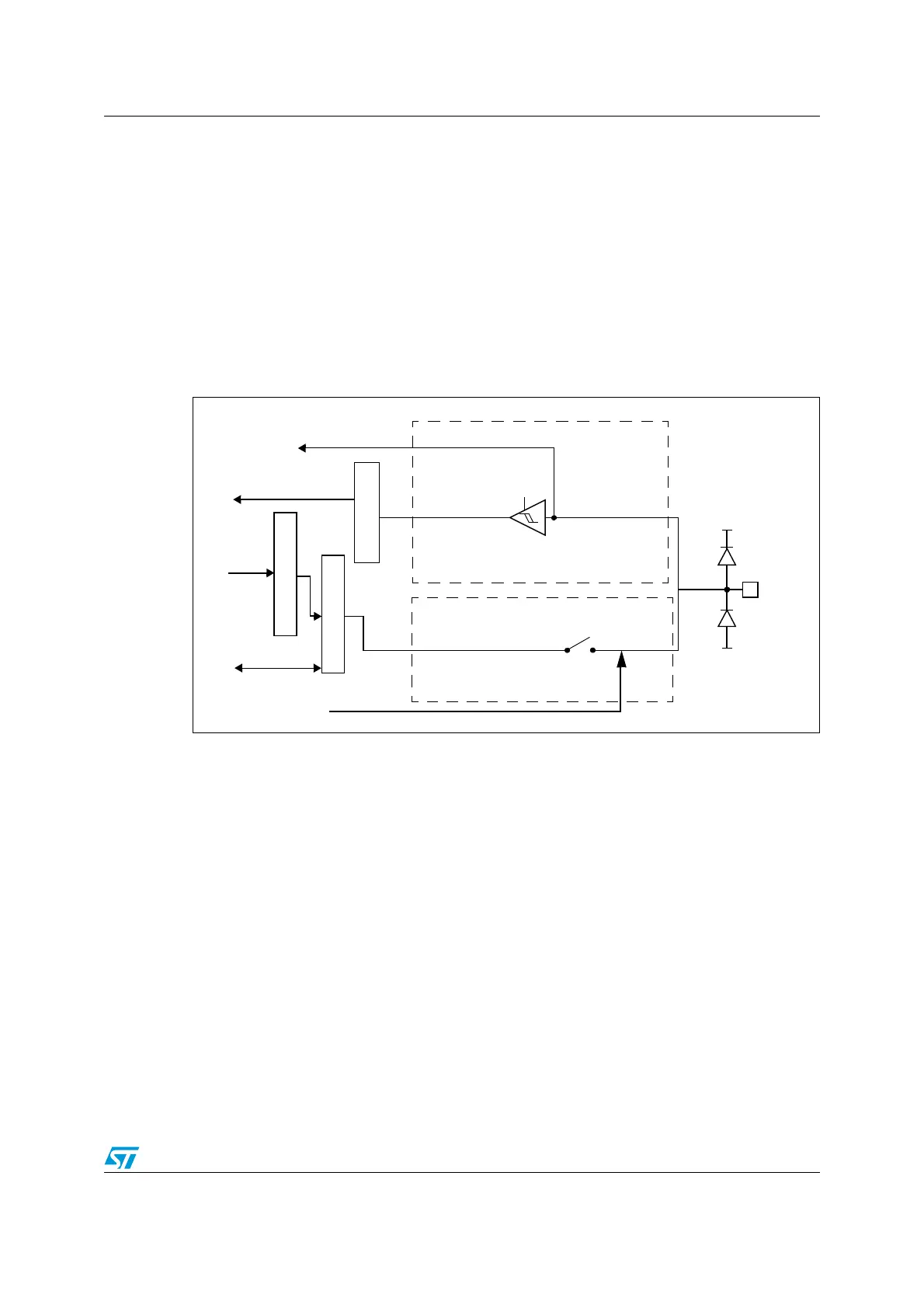
7.3.12 Analog configuration
When the I/O port is programmed as analog configuration:
● The output buffer is disabled
● The Schmitt trigger input is deactivated, providing zero consumption for every analog
value of the I/O pin. The output of the Schmitt trigger is forced to a constant value (0).
● The weak pull-up and pull-down resistors are disabled
● Read access to the input data register gets the value “0”
Note: In the analog configuration, the I/O pins cannot be 5 Volt tolerant.
Figure 23 shows the high-impedance, analog-input configuration of the I/O port bit.
Figure 23. High impedance-analog configuration
7.3.13 Using the OSC32_IN/OSC32_OUT pins as GPIO PC14/PC15
port pins
The LSE oscillator pins OSC32_IN and OSC32_OUT can be used as general-purpose
PC14 and PC15 I/Os, respectively, when the LSE oscillator is off. The PC14 and PC15 I/Os
are only configured as LSE oscillator pins OSC32_IN and OSC32_OUT when the LSE
oscillator is ON. This is done by setting the LSEON bit in the RCC_BDCR register. The LSE
has priority over the GPIO function.
Note: The PC14/PC15 GPIO functionality is lost when the 1.2 V domain is powered off (by the
device entering the standby mode) or when the backup domain is supplied by V
BAT
(V
DD
no
more supplied). In this case the I/Os are set in analog input mode.
7.3.14 Using the OSC_IN/OSC_OUT pins as GPIO PH0/PH1 port pins
The HSE oscillator pins OSC_IN/OSC_OUT can be used as general-purpose PH0/PH1
I/Os, respectively, when the HSE oscillator is OFF. (after reset, the HSE oscillator is off). The
PH0/PH1 I/Os are only configured as OSC_IN/OSC_OUT HSE oscillator pins when the
HSE oscillator is ON. This is done by setting the HSEON bit in the RCC_CR register. The
HSE has priority over the GPIO function.
From on-chip
peripheral
To on-chip
peripheral
Analog
trigger
off
Input driver
0
Input data register
Output data register
Read/write
Read
Bit set/reset registers
Write
Analog
V
SS
V
DD
protection
diode
protection
diode
I/O pin

 Loading...


