RM0090 Embedded Flash memory interface
Doc ID 018909 Rev 4 68/1422
Programming and caches
If a Flash memory write access concerns some data in the data cache, the Flash write
access modifies the data in the Flash memory and the data in the cache.
If an erase operation in Flash memory also concerns data in the data or instruction cache,
you have to make sure that these data are rewritten before they are accessed during code
execution. If this cannot be done safely, it is recommended to flush the caches by setting the
DCRST and ICRST bits in the FLASH_CR register.
Note: The I/D cache should be flushed only when it is disabled (I/DCEN = 0).
3.5.5 Interrupts
Setting the end of operation interrupt enable bit (EOPIE) in the FLASH_CR register enables
interrupt generation when an erase or program operation ends, that is when the busy bit
(BSY) in the FLASH_SR register is cleared (operation completed, correctly or not). In this
case, the end of operation (EOP) bit in the FLASH_SR register is set.
If an error occurs during a program, an erase, or a read operation request, one of the
following error flags is set in the FLASH_SR register:
● PGAERR, PGPERR, PGSERR (Program error flags)
● WRPERR (Protection error flag)
In this case, if the error interrupt enable bit (ERRIE) is set in the FLASH_SR register, an
interrupt is generated and the operation error bit (OPERR) is set in the FLASH_SR register.
Note: If several successive errors are detected (for example, in case of DMA transfer to the Flash
memory), the error flags cannot be cleared until the end of the successive write requests.
3.6 Option bytes
3.6.1 Description of user option bytes
The option bytes are configured by the end user depending on the application requirements.
Tabl e 1 0 shows the organization of these bytes inside the user configuration sector.
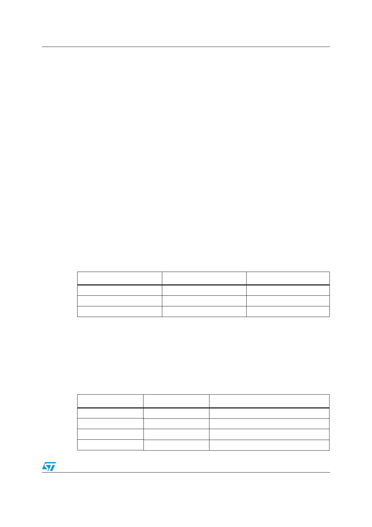
Table 9. Flash interrupt request
Interrupt event Event flag Enable control bit
End of operation EOP EOPIE
Write protection error WRPERR ERRIE
Programming error PGAERR, PGPERR, PGSERR ERRIE
Table 10. Option byte organization
Address [63:16] [15:0]
0x1FFF C000 Reserved ROP & user option bytes (RDP & USER)
0x1FFF C008 Reserved Write protection nWRP bits for sectors 0 to 11
0x1FFE C000 Reserved Reserved
0x1FFE C008 Reserved Write protection nWRP bits for sectors 12 to 23

 Loading...


