RM0090 General-purpose I/Os (GPIO)
Doc ID 018909 Rev 4 202/1422
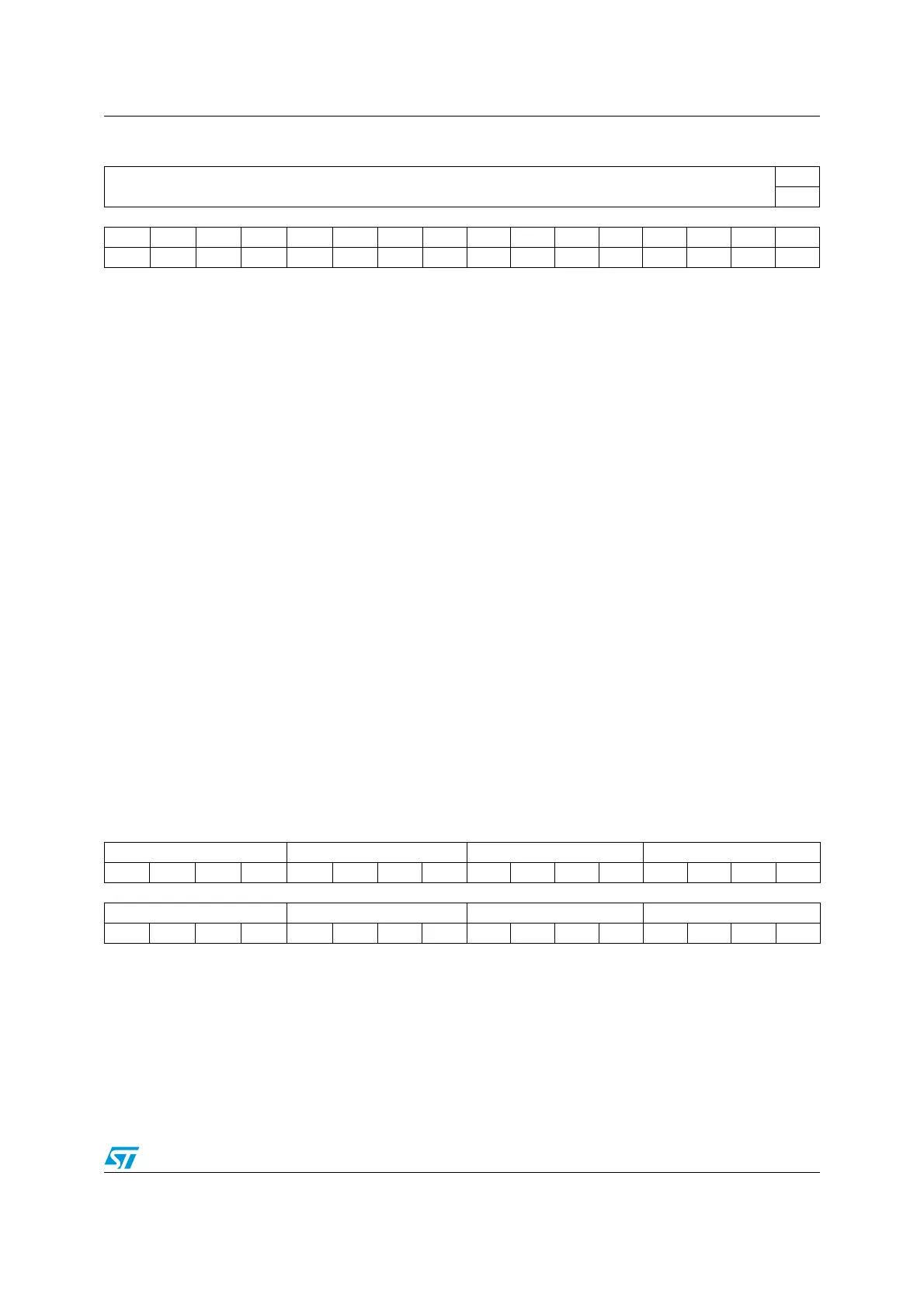
7.4.9 GPIO alternate function low register (GPIOx_AFRL) (x = A..I)
Address offset: 0x20
Reset value: 0x0000 0000
31 30 29 28 27 26 25 24 23 22 21 20 19 18 17 16
Reserved
LCKK
rw
15 14 13 12 11 10 9 8 7 6 5 4 3 2 1 0
LCK15 LCK14 LCK13 LCK12 LCK11 LCK10 LCK9 LCK8 LCK7 LCK6 LCK5 LCK4 LCK3 LCK2 LCK1 LCK0
rw rw rw rw rw rw rw rw rw rw rw rw rw rw rw rw
Bits 31:17 Reserved, must be kept at reset value.
Bit 16 LCKK[16]: Lock key
This bit can be read any time. It can only be modified using the lock key write sequence.
0: Port configuration lock key not active
1: Port configuration lock key active. The GPIOx_LCKR register is locked until an MCU reset
occurs.
LOCK key write sequence:
WR LCKR[16] = ‘1’ + LCKR[15:0]
WR LCKR[16] = ‘0’ + LCKR[15:0]
WR LCKR[16] = ‘1’ + LCKR[15:0]
RD LCKR
RD LCKR[16] = ‘1’ (this read operation is optional but it confirms that the lock is active)
Note: During the LOCK key write sequence, the value of LCK[15:0] must not change.
Any error in the lock sequence aborts the lock.
After the first lock sequence on any bit of the port, any read access on the LCKK bit will
return ‘1’ until the next CPU reset.
Bits 15:0 LCKy: Port x lock bit y (y= 0..15)
These bits are read/write but can only be written when the LCKK bit is ‘0.
0: Port configuration not locked
1: Port configuration locked
31 30 29 28 27 26 25 24 23 22 21 20 19 18 17 16
AFRL7[3:0] AFRL6[3:0] AFRL5[3:0] AFRL4[3:0]
rw rw rw rw rw rw rw rw rw rw rw rw rw rw rw rw
1514131211109876543210
AFRL3[3:0] AFRL2[3:0] AFRL1[3:0] AFRL0[3:0]
rw rw rw rw rw rw rw rw rw rw rw rw rw rw rw rw

 Loading...


