USB on-the-go high-speed (OTG_HS) RM0090
1179/1422 Doc ID 018909 Rev 4
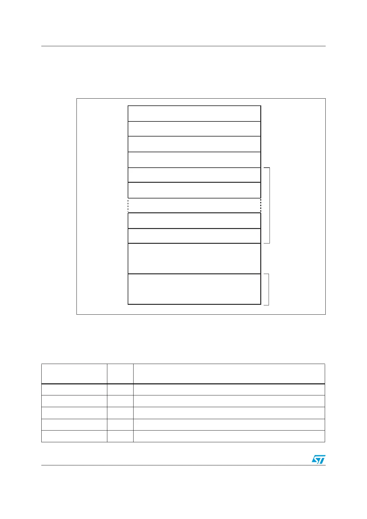
31.12.1 CSR memory map
The host and peripheral mode registers occupy different addresses. All registers are
implemented in the AHB clock domain.
Figure 384. CSR memory map
1. x = 5 in peripheral mode and x = 11 in host mode.
Global CSR map
These registers are available in both host and peripheral modes.
0000h
Core global CSRs (1 Kbyte)
0400h
Host mode CSRs (1 Kbyte)
0800h
Device mode CSRs (1.5 Kbyte)
0E00h
Power and clock gating CSRs (0.5 Kbyte)
1000h
Device EP 0/Host channel 0 FIFO (4 Kbyte)
2000h
Device EP1/Host channel 1 FIFO (4 Kbyte)
3000h
Device EP (x – 1)
(1)
/Host channel (x – 1)
(1)
FIFO (4 Kbyte)
Device EP x
(1)
/Host channel x
(1)
FIFO (4 Kbyte)
Reserved
DFIFO
push/pop
to this region
2 0000h
3 FFFFh
Direct access to data FIFO RAM
for debugging (128 Kbyte)
DFIFO
debug read/
write to this
region
ai15615b
Table 178. Core global control and status registers (CSRs)
Acronym
Address
offset
Register name
OTG_HS_GOTGCTL 0x000 OTG_HS control and status register (OTG_HS_GOTGCTL) on page 1184
OTG_HS_GOTGINT 0x004 OTG_HS interrupt register (OTG_HS_GOTGINT) on page 1186
OTG_HS_GAHBCFG 0x008 OTG_HS AHB configuration register (OTG_HS_GAHBCFG) on page 1187
OTG_HS_GUSBCFG 0x00C OTG_HS USB configuration register (OTG_HS_GUSBCFG) on page 1188
OTG_HS_GRSTCTL 0x010 OTG_HS reset register (OTG_HS_GRSTCTL) on page 1191

 Loading...


