Digital camera interface (DCMI) RM0090
331/1422 Doc ID 018909 Rev 4
13.5 DCMI functional overview
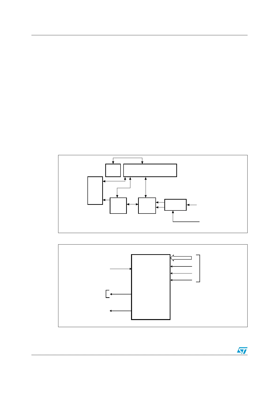
The digital camera interface is a synchronous parallel interface that can receive high-speed
(up to 54 Mbytes/s) data flows. It consists of up to 14 data lines (D13-D0) and a pixel clock
line (PIXCLK). The pixel clock has a programmable polarity, so that data can be captured on
either the rising or the falling edge of the pixel clock.
The data are packed into a 32-bit data register (DCMI_DR) and then transferred through a
general-purpose DMA channel. The image buffer is managed by the DMA, not by the
camera interface.
The data received from the camera can be organized in lines/frames (raw YUB/RGB/Bayer
modes) or can be a sequence of JPEG images. To enable JPEG image reception, the JPEG
bit (bit 3 of DCMI_CR register) must be set.
The data flow is synchronized either by hardware using the optional HSYNC (horizontal
synchronization) and VSYNC (vertical synchronization) signals or by synchronization codes
embedded in the data flow.
Figure 62 shows the DCMI block diagram.
Figure 62. DCMI block diagram
Figure 63. Top-level block diagram
DMA
interface
Control/Status
register
AHB
interface
FIFO/
Data
formatter
Data
extraction
Synchronizer
DCMI_PIXCLK
DCMI_D[0:13], DCMI_HSYNC, DCMI_VSYNC
ai15604
DCMI
Interrupt
controller
DCMI_IT
External
interface
DCMI_D[0:13]
DCMI_PIXCLK
DCMI_HSYNC
DCMI_VSYNC
DMA_REQ
HCLK
ai15603b