Secure digital input/output interface (SDIO) RM0090
887/1422 Doc ID 018909 Rev 4
28.9 SDIO registers
The device communicates to the system via 32-bit-wide control registers accessible via
APB2.
The peripheral registers have to be accessed by words (32 bits).
28.9.1 SDIO power control register (SDIO_POWER)
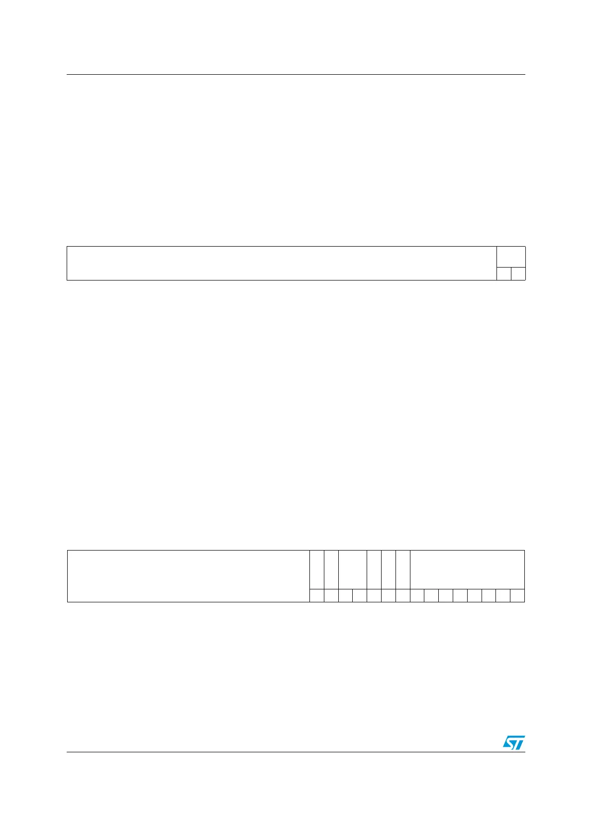
Address offset: 0x00
Reset value: 0x0000 0000
Note: At least seven HCLK clock periods are needed between two write accesses to this register.
Note: After a data write, data cannot be written to this register for three SDIOCLK (48 MHz) clock
periods plus two PCLK2 clock periods.
28.9.2 SDI clock control register (SDIO_CLKCR)
Address offset: 0x04
Reset value: 0x0000 0000
The SDIO_CLKCR register controls the SDIO_CK output clock.
313029282726252423222120191817161514131211109876543210
Reserved
PWRC
TRL
rw rw
Bits 31:2 Reserved, must be kept at reset value
Bits 1:0 PWRCTRL: Power supply control bits.
These bits are used to define the current functional state of the card clock:
00: Power-off: the clock to card is stopped.
01: Reserved
10: Reserved power-up
11: Power-on: the card is clocked.
313029282726252423222120191817161514131211109876543210
Reserved
HWFC_EN
NEGEDGE
WID
BUS
BYPASS
PWRSAV
CLKEN
CLKDIV
rw rw rw rw rw rw rw rw rw rw rw rw rw rw rw

 Loading...


