Flexible static memory controller (FSMC) RM0090
1361/1422 Doc ID 018909 Rev 4
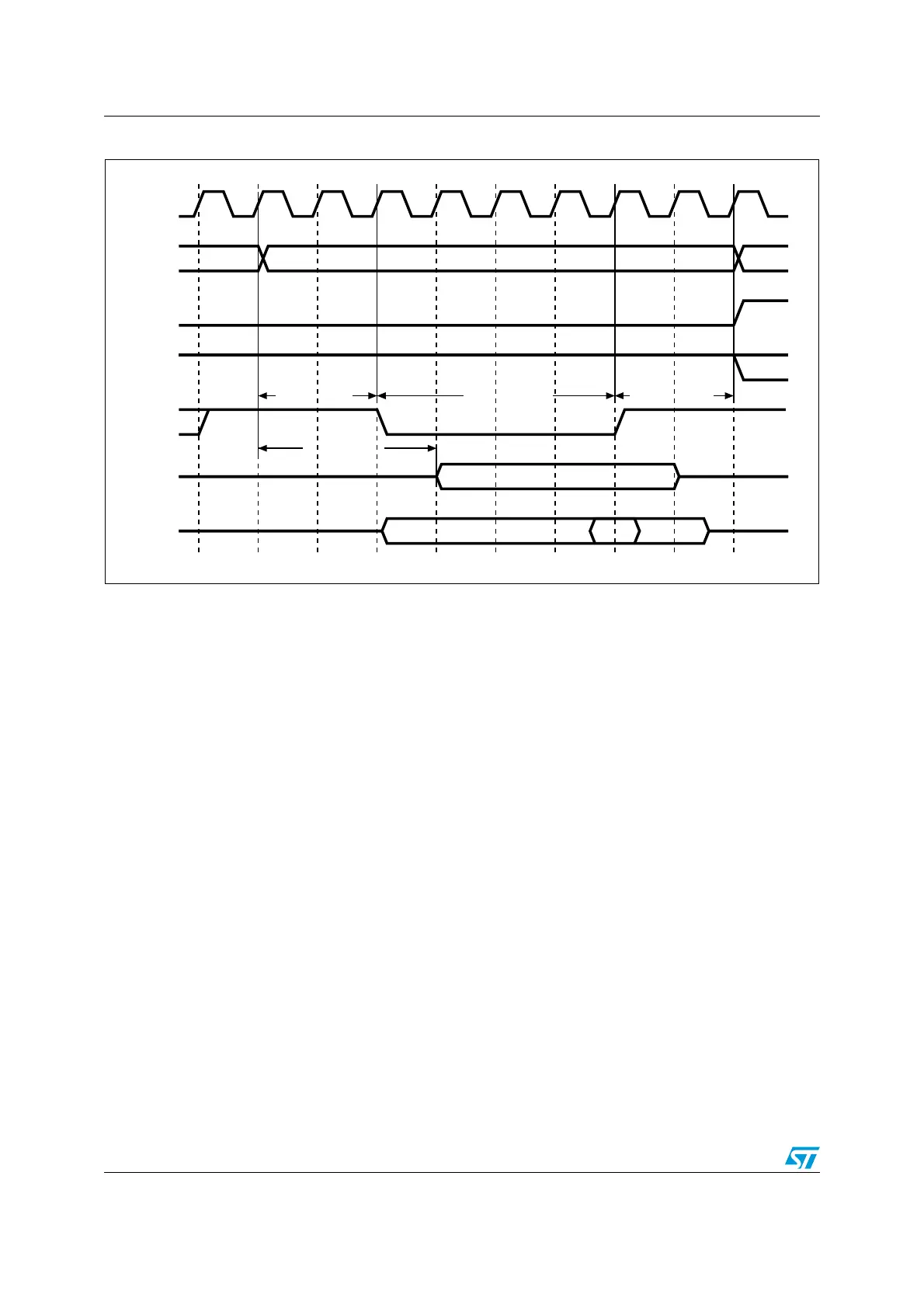
Figure 423. NAND/PC Card controller timing for common memory access
1. NOE remains high (inactive) during write access. NWE remains high (inactive) during read access.
32.6.4 NAND Flash operations
The command latch enable (CLE) and address latch enable (ALE) signals of the NAND
Flash device are driven by some address signals of the FSMC controller. This means that to
send a command or an address to the NAND Flash memory, the CPU has to perform a write
to a certain address in its memory space.
A typical page read operation from the NAND Flash device is as follows:
1. Program and enable the corresponding memory bank by configuring the FSMC_PCRx
and FSMC_PMEMx (and for some devices, FSMC_PATTx, see Section 32.6.5: NAND
Flash pre-wait functionality on page 1362) registers according to the characteristics of
the NAND Flash (PWID bits for the databus width of the NAND Flash, PTYP = 1,
PWAITEN = 1, PBKEN = 1, see section Common memory space timing register 2..4
(FSMC_PMEM2..4) on page 1368 for timing configuration).
2. The CPU performs a byte write in the common memory space, with data byte equal to
one Flash command byte (for example 0x00 for Samsung NAND Flash devices). The
CLE input of the NAND Flash is active during the write strobe (low pulse on NWE), thus
the written byte is interpreted as a command by the NAND Flash. Once the command
is latched by the NAND Flash device, it does not need to be written for the following
page read operations.
3. The CPU can send the start address (STARTAD) for a read operation by writing the
required bytes (for example four bytes or three for smaller capacity devices),
STARTAD[7:0], STARTAD[15:8], STARTAD[23:16] and finally STARTAD[25:24] for
64 Mb x 8 bit NAND Flash) in the common memory or attribute space. The ALE input of
the NAND Flash device is active during the write strobe (low pulse on NWE), thus the
written bytes are interpreted as the start address for read operations. Using the
i15570b
HCLK
A[25:0]
NCEx
NREG,
NIOW,
NIOR
NWE,
NOE
(1)
write_data
read_data
High
Valid
MEMxSET + 1
MEMxWAIT + 1
MEMxHOLD + 1
MEMxHIZ

 Loading...


