Memory and bus architecture RM0090
57/1422 Doc ID 018909 Rev 4
BOOT0 is a dedicated pin while BOOT1 is shared with a GPIO pin. Once BOOT1 has been
sampled, the corresponding GPIO pin is free and can be used for other purposes.
The BOOT pins are also resampled when the device exits the Standby mode. Consequently,
they must be kept in the required Boot mode configuration when the device is in the Standby
mode. After this startup delay is over, the CPU fetches the top-of-stack value from address
0x0000 0000, then starts code execution from the boot memory starting from 0x0000 0004.
Note: When the device boots from SRAM, in the application initialization code, you have to
relocate the vector table in SRAM using the NVIC exception table and the offset register.
Embedded bootloader
The embedded bootloader mode is used to reprogram the Flash memory using one of the
following serial interfaces:
● USART1(PA9/PA10)
● USART3(PB10/11 and PC10/11)
● CAN2(PB5/13)
● USB OTG FS(PA11/12) in Device mode (DFU: device firmware upgrade).
The USART peripherals operate at the internal 16 MHz oscillator (HSI) frequency, while the
CAN and USB OTG FS require an external clock (HSE) multiple of 1 MHz (ranging from 4 to
26 MHz).
The embedded bootloader code is located in system memory. It is programmed by ST
during production. For additional information, refer to application note AN2606.
Physical remap
Once the boot pins are selected, the application software can modify the memory
accessible in the code area (in this way the code can be executed through the ICode bus in
place of the System bus). This modification is performed by programming the Section 8.2.1:
SYSCFG memory remap register (SYSCFG_MEMRMP) in the SYSCFG controller.
The following memories can thus be remapped:
● Main Flash memory
● System memory
● Embedded SRAM1 (112 KB)
● FSMC bank 1 (NOR/PSRAM 1 and 2)
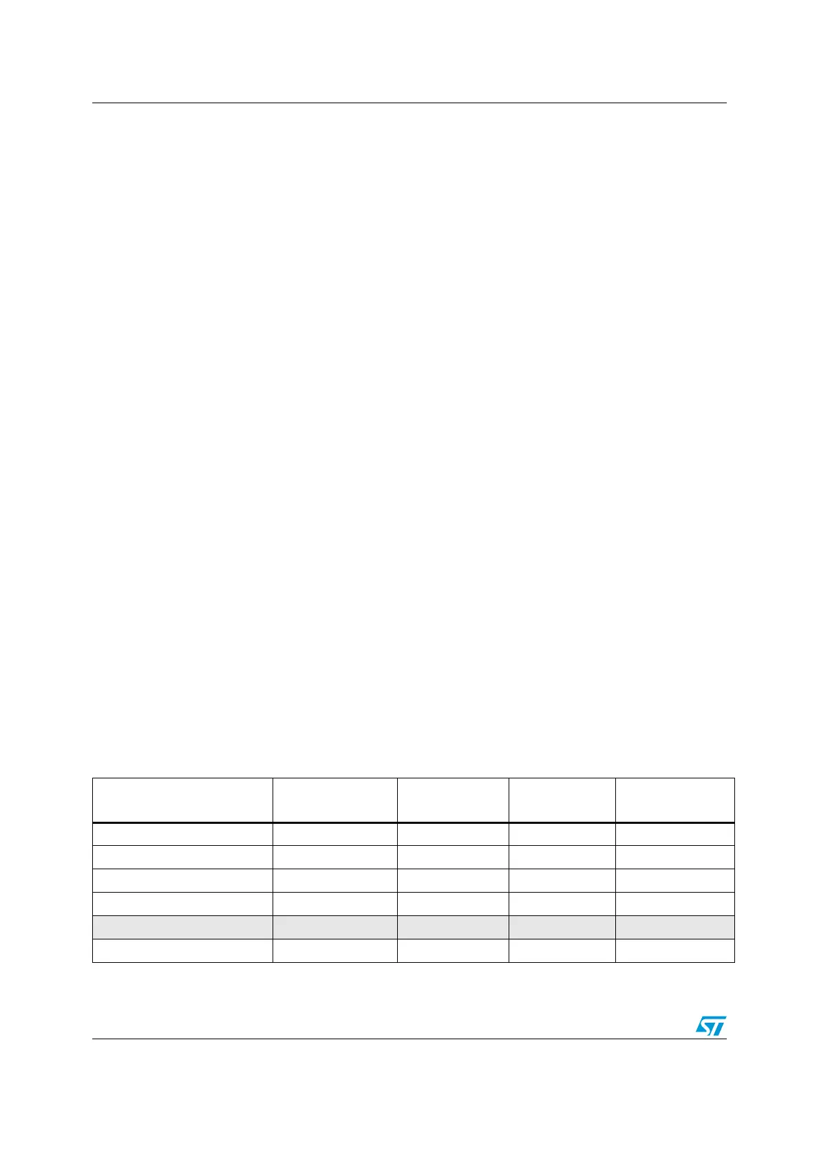
Table 4. Memory mapping vs. Boot mode/physical remap
Addresses
Boot/Remap in
main Flash memory
Boot/Remap in
embedded SRAM
Boot/Remap in
System memory
Remap in FSMC
0x2002 0000 - 0x2002 FFFF
(1)
SRAM3 (64 KB) SRAM3 (64 KB) SRAM3 (64 KB) SRAM3 (64 KB)
0x2001 C000 - 0x2001 FFFF SRAM2 (16 KB) SRAM2 (16 KB) SRAM2 (16 KB) SRAM2 (16 KB)
0x2000 0000 - 0x2001 BFFF SRAM1 (112 KB) SRAM1 (112 KB) SRAM1 (112 KB) SRAM1 (112 KB)
0x1FFF 0000 - 0x1FFF 77FF System memory System memory System memory System memory
0x0810 0000 - 0x0FFF FFFF Reserved Reserved Reserved Reserved
0x0800 0000 - 0x080F FFFF Flash memory Flash memory Flash memory Flash memory

 Loading...


