RM0090 Debug support (DBG)
Doc ID 018909 Rev 4 1406/1422
33.17.10 Example of configuration
● Set the bit TRCENA in the Debug Exception and Monitor Control Register (DEMCR)
● Write the TPIU Current Port Size Register to the desired value (default is 0x1 for a 1-bit
port size)
● Write TPIU Formatter and Flush Control Register to 0x102 (default value)
● Write the TPIU Select Pin Protocol to select the sync or async mode. Example: 0x2 for
async NRZ mode (UART like)
● Write the DBGMCU control register to 0x20 (bit IO_TRACEN) to assign TRACE I/Os for
async mode. A TPIU Sync packet is emitted at this time (FF_FF_FF_7F)
● Configure the ITM and write the ITM Stimulus register to output a value
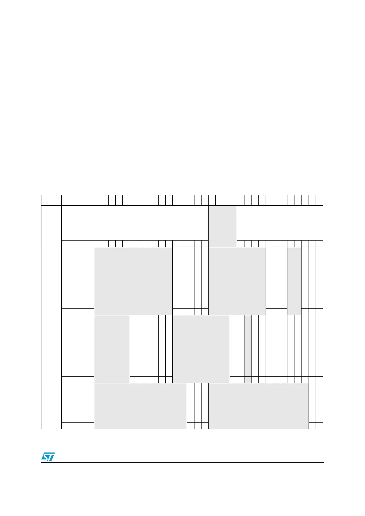
33.18 DBG register map
The following table summarizes the Debug registers
.
Table 239. DBG register map and reset values
Addr. Register
31
30
29
28
27
26
25
24
23
22
21
20
19
18
17
16
15
14
13
12
11
10
9
8
7
6
5
4
3
2
1
0
0xE004
2000
DBGMCU_IDC
ODE
REV_ID
Reserved
DEV_ID
Reset value
(1)
XX XX XX XX XX XX XX XX XX XX XX XX XX XX
0xE004
2004
DBGMCU_CR
Reserved
DBG_TIM7_STOP
DBG_TIM6_STOP
DBG_TIM5_STOP
DBG_TIM8_STOP
DBG_I2C2_SMBUS_TIMEOUT
Reserved
TRAC
E_
MODE
[1:0]
TR
AC
E_
IO
E
N
Reserved
DBG_STANDBY
DBG_STOP
DBG_SLEEP
Reset value 00000 000 000
0xE004
2008
DBGMCU_
APB1_FZ
Reserved
DBG_CAN2_STOP
DBG_CAN1_STOP
Reserved
DBG_I2C3_SMBUS_TIMEOUT
DBG_I2C2_SMBUS_TIMEOUT
DBG_I2C1_SMBUS_TIMEOUT
Reserved
DBG_IWDG_STOP
DBG_WWDG_STOP
Reserved
DBG_RTC_STOP
DBG_TIM14_STOP
DBG_TIM13_STOP
DBG_TIM12_STOP
DBG_TIM7_STOP
DBG_TIM6_STOP
DBG_TIM5_STOP
DBG_TIM4_STOP
DBG_TIM3_STOP
DBG_TIM2_STOP
Reset value 000000 00 0000000000
0xE004
200C
DBGMCU_
APB2_FZ
Reserved
DBG_TIM11_STOP
DBG_TIM10_STOP
DBG_TIM9_STOP
Reserved
DBG_TIM8_STOP
DBG_TIM1_STOP
Reset value 000 00
1. The reset value is product dependent. For more information, refer to Section 33.6.1: MCU device ID code.

 Loading...


