Reset and clock control for (RCC) RM0090
125/1422 Doc ID 018909 Rev 4
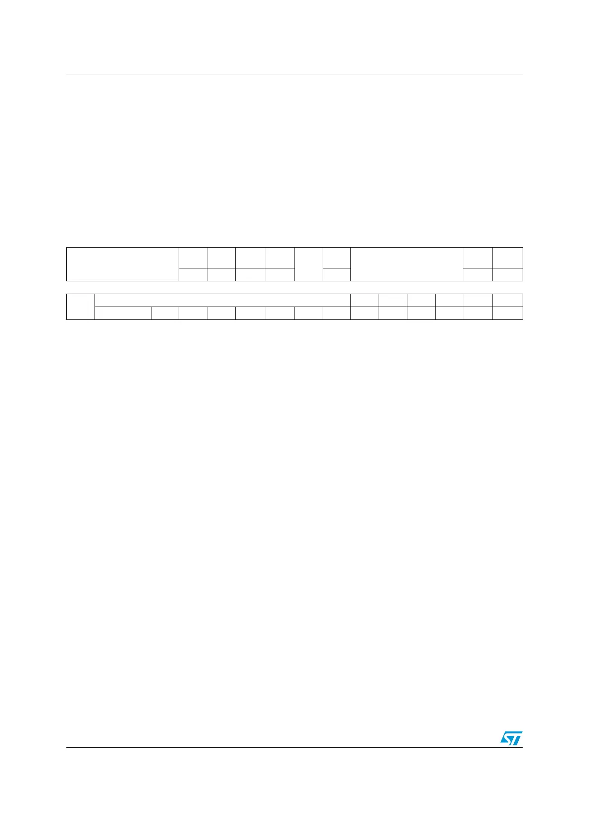
6.3.2 RCC PLL configuration register (RCC_PLLCFGR)
Address offset: 0x04
Reset value: 0x2400 3010
Access: no wait state, word, half-word and byte access.
This register is used to configure the PLL clock outputs according to the formulas:
● f
(VCO clock)
= f
(PLL clock input)
× (PLLN / PLLM)
● f
(PLL general clock output)
= f
(VCO clock)
/ PLLP
● f
(USB OTG FS, SDIO, RNG clock output)
= f
(VCO clock)
/ PLLQ
31 30 29 28 27 26 25 24 23 22 21 20 19 18 17 16
Reserved
PLLQ3 PLLQ2 PLLQ1 PLLQ0
Reserv
ed
PLLSR
C
Reserved
PLLP1 PLLP0
rw rw rw rw rw rw rw
15 14 13 12 11 10 9 8 7 6 5 4 3 2 1 0
Reserv
ed
PLLN PLLM5 PLLM4 PLLM3 PLLM2 PLLM1 PLLM0
rw rw rw rw rw rw rw rw rw rw rw rw rw rw rw
Bit 31:28 Reserved, must be kept at reset value.
Bits 27:24 PLLQ: Main PLL (PLL) division factor for USB OTG FS, SDIO and random number generator
clocks
Set and cleared by software to control the frequency of USB OTG FS clock, the random
number generator clock and the SDIO clock. These bits should be written only if PLL is
disabled.
Caution: The USB OTG FS requires a 48 MHz clock to work correctly. The SDIO and the
random number generator need a frequency lower than or equal to 48 MHz to work
correctly.
USB OTG FS clock frequency = VCO frequency / PLLQ with 2 ≤ PLLQ ≤ 15
0000: PLLQ = 0, wrong configuration
0001: PLLQ = 1, wrong configuration
0010: PLLQ = 2
0011: PLLQ = 3
0100: PLLQ = 4
...
1111: PLLQ = 15
Bit 23 Reserved, must be kept at reset value.
Bit 22 PLLSRC: Main PLL(PLL) and audio PLL (PLLI2S) entry clock source
Set and cleared by software to select PLL and PLLI2S clock source. This bit can be written
only when PLL and PLLI2S are disabled.
0: HSI clock selected as PLL and PLLI2S clock entry
1: HSE oscillator clock selected as PLL and PLLI2S clock entry
Bits 21:18 Reserved, must be kept at reset value.

 Loading...


