RM0090 Inter-integrated circuit (I
2
C) interface
Doc ID 018909 Rev 4 710/1422
A 9th clock pulse follows the 8 clock cycles of a byte transfer, during which the receiver must
send an acknowledge bit to the transmitter. Refer to Figure 238.
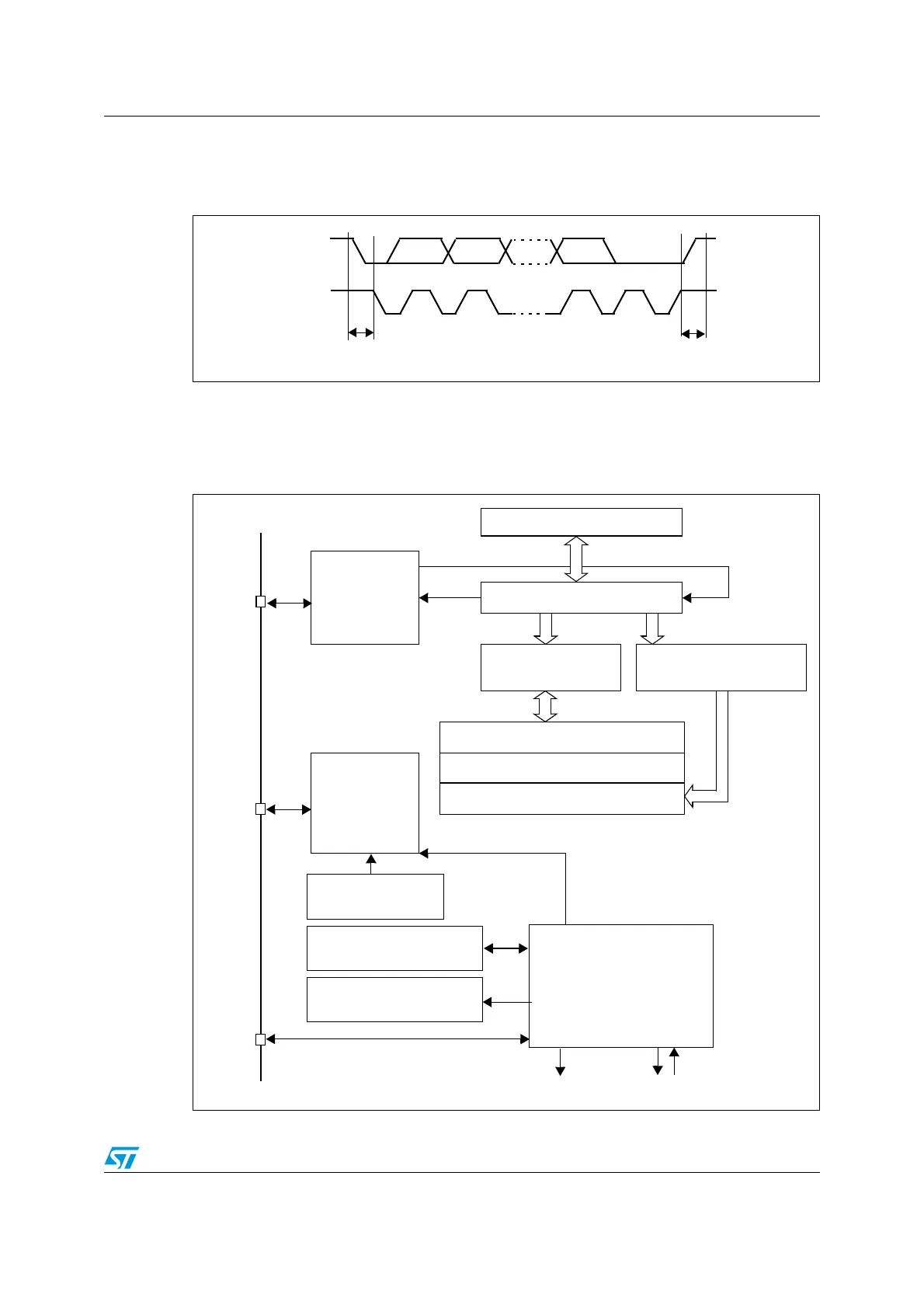
Figure 238. I
2
C bus protocol
Acknowledge may be enabled or disabled by software. The I
2
C interface addresses (dual
addressing 7-bit/ 10-bit and/or general call address) can be selected by software.
The block diagram of the I
2
C interface is shown in Figure 239.
Figure 239. I
2
C block diagram for STM32F40x/41x
SCL
SDA
12 8 9
MSB
ACK
Stop
Start
condition
condition
Data shift register
Comparator
Own address register
Clock control
Status registers
Control registers
Control
Clock
control
Data
control
SCL
logic
Dual address register
Data register
PEC register
Interrupts
PEC calculation
SMBA
SDA
Register (CCR)
(SR1&SR2)
(CR1&CR2)
DMA requests & ACK

 Loading...


