RM0090 Analog-to-digital converter (ADC)
Doc ID 018909 Rev 4 278/1422
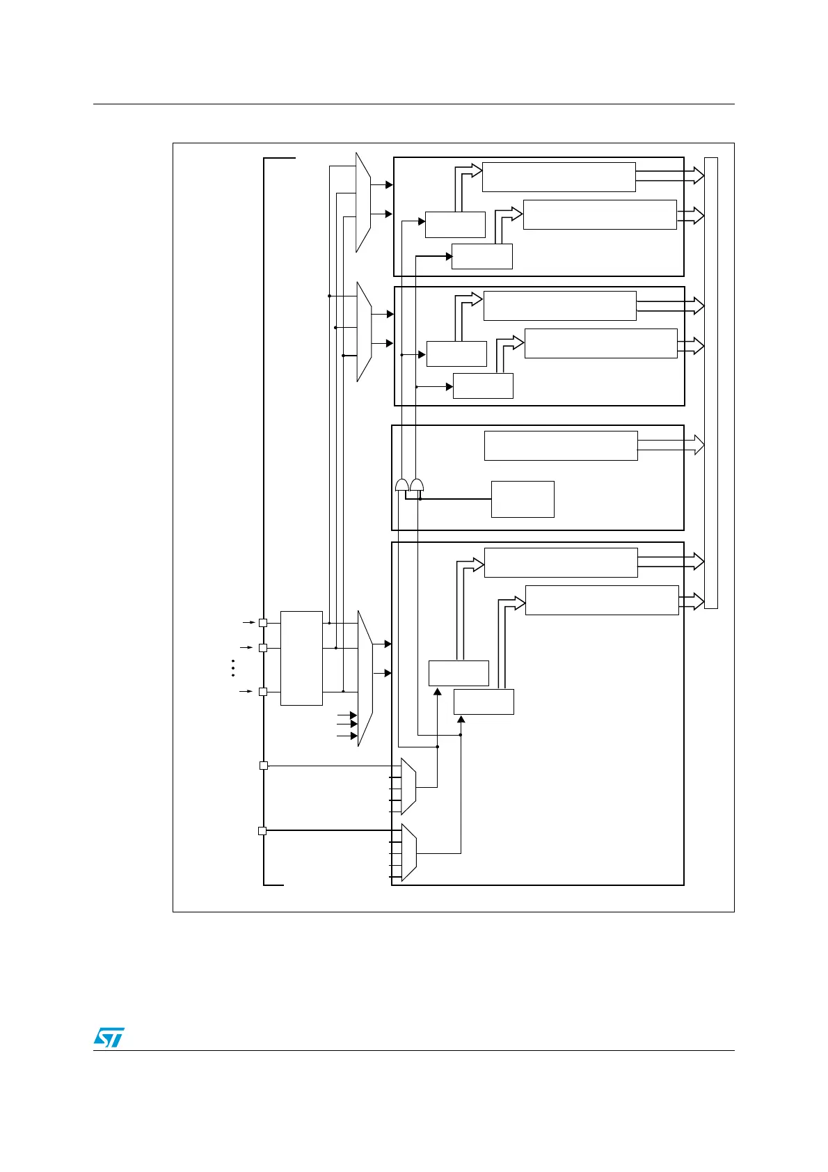
Figure 41. Multi ADC block diagram
(1)
1. Although external triggers are present on ADC2 and ADC3 they are not shown in this diagram.
2. In the Dual ADC mode, the ADC3 slave part is not present.
3. In Triple ADC mode, the ADC common data register (ADC_CDR) contains the ADC1, ADC2 and ADC3’s
regular converted data. All 32 register bits are used according to a selected storage order.
In Dual ADC mode, the ADC common data register (ADC_CDR) contains both the ADC1 and ADC2’s
regular converted data. All 32 register bits are used.
ADCx_IN0
ADCx_IN1
ADCx_IN15
GPIO
Ports
Address/data bus
EXTI_11
EXTI_15
Injected data registers
(4 x 16 bits)
Regular
channels
Injected
channels
ADC3
(2)
(Slave)
(12 bits)
Injected data registers
(4 x 16 bits)
Regular
channels
Injected
channels
ADC1 (Master)
Dual/Triple
internal triggers
Start trigger mux
(regular group)
(injected group)
Start trigger mux
control
Temp. sensor
V
REFINT
Regular data register
(16 bits)
Regular data register
(16 bits)
Common regular data register
(32 bits)
(3)
V
BAT
Common part
mode
ADC2 (Slave)
(12 bits)
Injected data registers
(4 x 16 bits)
Regular
channels
Injected
channels
Regular data register
(16 bits)
ai16053

 Loading...


