RM0090 Universal synchronous asynchronous receiver transmitter (USART)
Doc ID 018909 Rev 4 772/1422
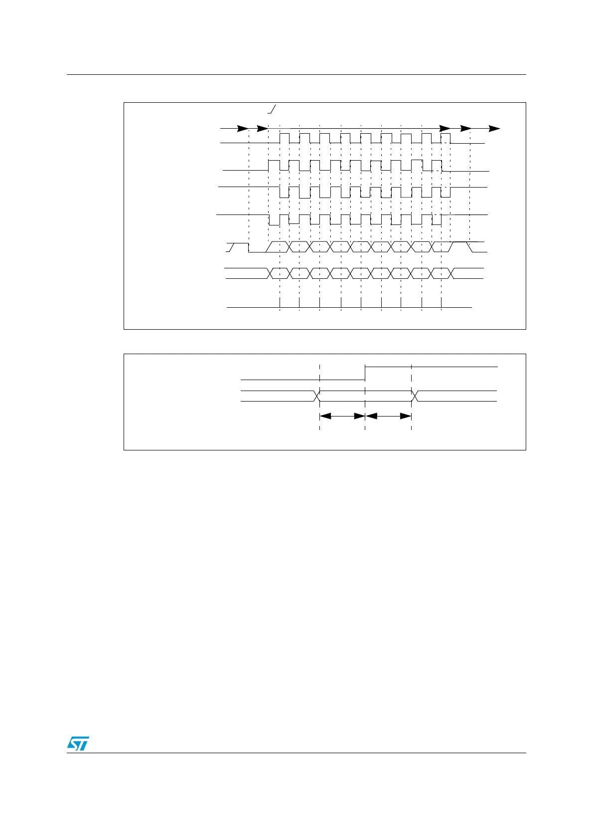
Figure 259. USART data clock timing diagram (M=1)
Figure 260. RX data setup/hold time
Note: The function of SCLK is different in Smartcard mode. Refer to the Smartcard mode chapter
for more details.
26.3.10 Single-wire half-duplex communication
The single-wire half-duplex mode is selected by setting the HDSEL bit in the USART_CR3
register. In this mode, the following bits must be kept cleared:
● LINEN and CLKEN bits in the USART_CR2 register,
● SCEN and IREN bits in the USART_CR3 register.
The USART can be configured to follow a single-wire half-duplex protocol where the TX and
RX lines are internally connected. The selection between half- and full-duplex
communication is made with a control bit ‘HALF DUPLEX SEL’ (HDSEL in USART_CR3).
As soon as HDSEL is written to 1:
● the TX and RX lines are internally connected
● the RX pin is no longer used
● the TX pin is always released when no data is transmitted. Thus, it acts as a standard
I/O in idle or in reception. It means that the I/O must be configured so that TX is
configured as floating input (or output high open-drain) when not driven by the USART.
Idle or next
M=1 (9 data bits)
Clock (CPOL=0, CPHA=1)
Clock (CPOL=1, CPHA=0)
Clock (CPOL=1, CPHA=1)
Start LSB
MSB Stop
* LBCL bit controls last data clock pulse
Start
Idle or preceding
transmission
Data on TX
Stop
Clock (CPOL=0, CPHA=0)
01 23456 7
*
*
*
*
8
transmission
Capture Strobe
LSB
MSB
Data on RX
01 23456 7
(from slave)
(from master)
*
8
valid DATA bit
t
SETUP
t
HOLD
SCLK (capture strobe on SCLK
rising edge in this example)
Data on RX
(from slave)
t
SETUP
= t
HOLD
1/16 bit time

 Loading...


