RM0090 Embedded Flash memory interface
Doc ID 018909 Rev 4 80/1422
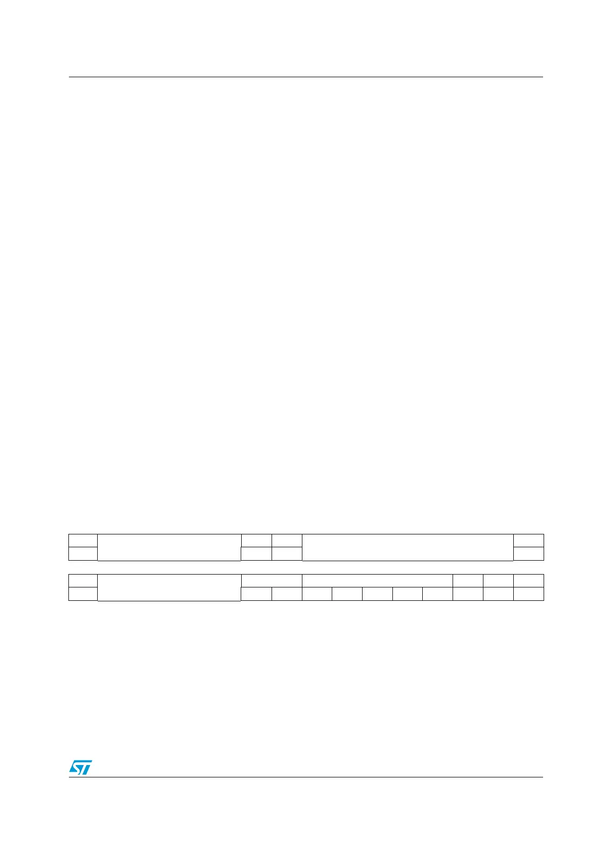
3.8.6 Flash control register (FLASH_CR) for
STM32F42xxx and STM32F43xxx
The Flash control register is used to configure and start Flash memory operations.
Address offset: 0x10
Reset value: 0x8000 0000
Access: no wait state when no Flash memory operation is ongoing, word, half-word and
byte access.
Bits 15:10 Reserved, must be kept cleared.
Bits 9:8 PSIZE: Program size
These bits select the program parallelism.
00 program x8
01 program x16
10 program x32
11 program x64
Bits 6:3 SNB: Sector number
These bits select the sector to erase.
0000 sector 0
0001 sector 1
...
1011 sector 11
Others not allowed
Bit 2 MER: Mass Erase
Erase activated for all user sectors.
Bit 1 SER: Sector Erase
Sector Erase activated.
Bit 0 PG: Programming
Flash programming activated.
31 30 29 28 27 26 25 24 23 22 21 20 19 18 17 16
LOCK
Reserved
ERRIE EOPIE
Reserved
STRT
rs rw rw rs
15 14 13 12 11 10 9 8 7 6 5 4 3 2 1 0
MER1
Reserved
PSIZE[1:0] SNB[4:0] MER SER PG
rw rw rw rw rw rw rw rw rw rw rw

 Loading...


