RM0090 USB on-the-go high-speed (OTG_HS)
Doc ID 018909 Rev 4 1162/1422
31.3 OTG_HS functional description
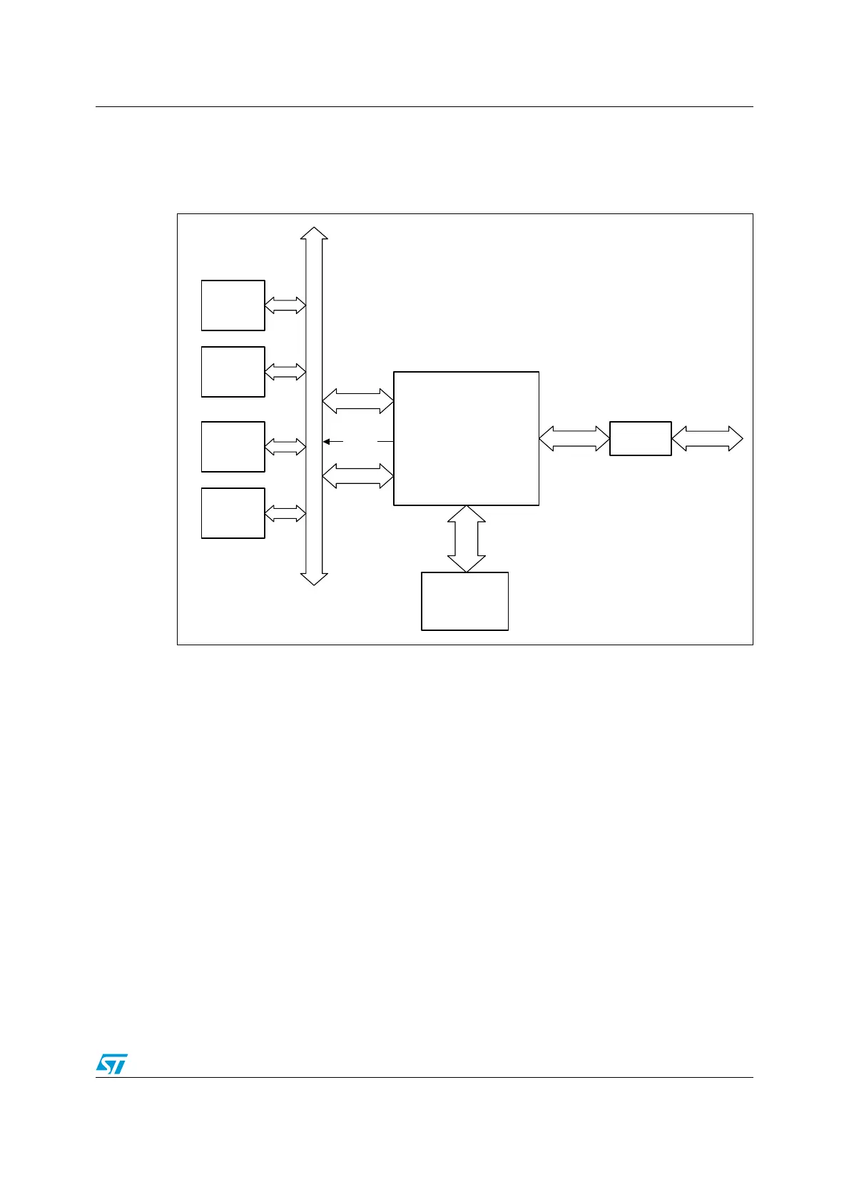
Figure 381 shows the OTG_HS interface block diagram.
Figure 381. USB OTG interface block diagram
1. The USB DMA cannot directly address the internal Flash memory.
31.3.1 High-speed OTG PHY
The USB OTG HS core embeds an ULPI interface to connect an external HS phy.
31.3.2 External Full-speed OTG PHY using the I2C interface
The USB OTG HS core embeds an I
2
C interface allowing to connect an external FS phy.
31.3.3 Embedded Full-speed OTG PHY
The full-speed OTG PHY includes the following components:
● FS/LS transceiver module used by both host and Device. It directly drives transmission
and reception on the single-ended USB lines.
● Integrated ID pull-up resistor used to sample the ID line for A/B Device identification.
● DP/DM integrated pull-up and pull-down resistors controlled by the OTG_HS core
depending on the current role of the device. As a peripheral, it enables the DP pull-up
resistor to signal full-speed peripheral connections as soon as V
BUS
is sensed to be at
a valid level (B-session valid). In host mode, pull-down resistors are enabled on both
AHB master interface
AHB slave interface
CPU
Memory
Peripheral 1
Peripheral 2
ULPI interface
ULPI PHY
2.0 USB
Data FIFO
single-port RAM
(SPRAM)
Data FIFO
RAM interface
Interrupt
AHB (application bus)
USB OTG HS core
ai17107b

 Loading...


