MPC5604B/C Microcontroller Reference Manual, Rev. 8
Freescale Semiconductor 103
NOTE
The user must take care not to program device with a frequency higher than
allowed (no hardware check).
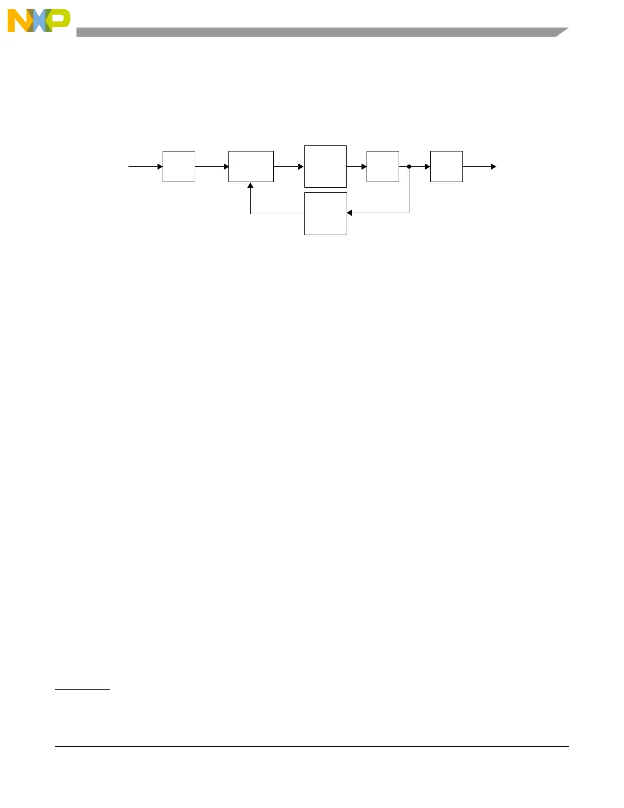
The FMPLL block diagram is shown in Figure 6-6.
Figure 6-6. FMPLL block diagram
6.7.3 Features
The FMPLL has the following major features:
• Input clock frequency 4 MHz – 16 MHz
• Voltage controlled oscillator (VCO) range from 256 MHz to 512 MHz
• Frequency divider (FD) for reduced frequency operation without forcing the FMPLL to relock
• Frequency modulated FMPLL
— Modulation enabled/disabled through software
— Triangle wave modulation
• Programmable modulation depth
— ±0.25% to ±4% deviation from center spread frequency
1
— 0.5% to +8% deviation from down spread frequency
— Programmable modulation frequency dependent on reference frequency
• Self-clocked mode (SCM) operation
• 4 available modes
— Normal mode
— Progressive clock switching
— Normal mode with frequency modulation
— Powerdown mode
6.7.4 Memory map
2
Table 6-8 shows the memory map of the FMPLL.
1. Spread spectrum should be programmed in line with maximum datasheet frequency figures.
2. FMPLL_x are mapped through the ME_CGM register slot
BUFFER
Charge
Pump
Low Pass
Filter
VCOIDF
NDIV
Loop
Frequency
Divider
ODF
PHI
FXOSC
 Loading...