MPC5604B/C Microcontroller Reference Manual, Rev. 8
Freescale Semiconductor 627
25.4.8 Delay registers
25.4.8.1 Decode Signals Delay Register (DSDR)
25.4.8.2 Power-down Exit Delay Register (PDEDR)
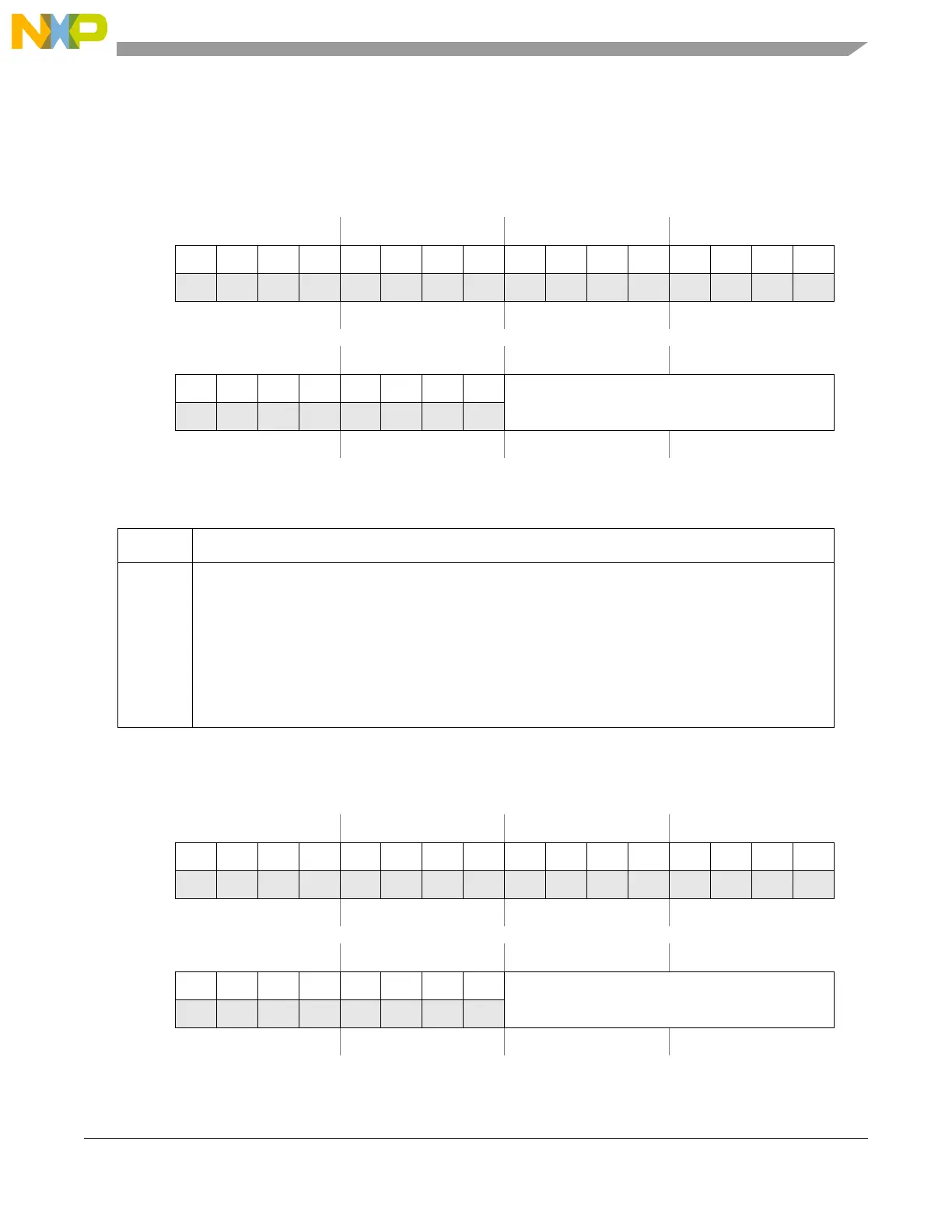
Address:
Base + 0x00C4 Access: User read/write
0123456789101112131415
R00000000 00000 000
W
Reset0000000000000000
16 17 18 19 20 21 22 23 24 25 26 27 28 29 30 31
R00000000
DSD
W
Reset0000000000000000
Figure 25-33. Decode Signals Delay Register (DSDR)
Table 25-22. DSDR field descriptions
Field Description
DSD Delay between the external decode signals and the start of the sampling phase
It is used to take into account the settling time of the external multiplexer.
The decode signal delay is calculated as: DSD × 1/frequency of ADC clock.
Note: when ADC clock = Peripheral Clock/2 the DSD has to be incremented by 2 to see an additional
ADC clock cycle delay on the decode signal.
For example:
DSD = 0; 0 ADC clock cycle delay
DSD = 2; 1 ADC clock cycle delay
DSD = 4; 2 ADC clock cycles delay
Address:
Base + 0x00C8 Access: User read/write
0123456789101112131415
R00000000 00000 000
W
Reset0000000000000000
16 17 18 19 20 21 22 23 24 25 26 27 28 29 30 31
R00000000
PDED
W
Reset0000000000000000
Figure 25-34. Power-down Exit Delay Register (PDEDR)