MPC5604B/C Microcontroller Reference Manual, Rev. 8
Freescale Semiconductor 643
The division into blocks of the flash memory module is also used to implement independent erase/program
protection. A software mechanism is provided to independently lock/unlock each block in low and mid
address space against program and erase.
27.4.2.2 DFlash module sectorization
The DFlash module supports 64 KB of user memory, plus 16 KB of test memory (a portion of which is
One-Time Programmable by the user).
The module is composed of a single bank (Bank 0): Read-While-Write is not supported.
Bank 0 of the 80 KB module is divided in four sectors. Bank 0 also contains a reserved sector named
TestFlash in which some One-Time Programmable user data are stored.
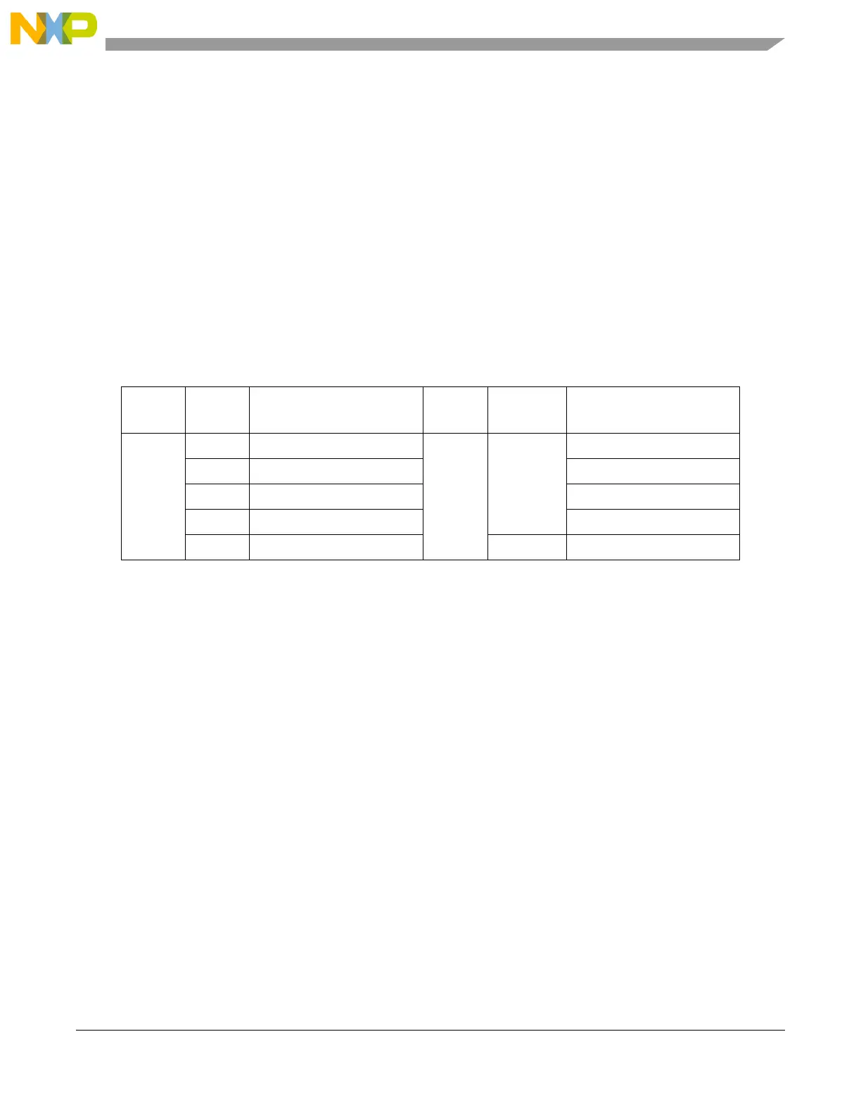
The sectorization of the 80 KB matrix module is shown in Table 27-3.
The flash memory module is divided into blocks also to implement independent erase/program protection.
A software mechanism is provided to independently lock/unlock each block in low and mid address space
against program and erase.
27.4.3 TestFlash block
A TestFlash block is available in both the CFlash and DFlash modules. The TestFlash block exists outside
the normal address space and is programmed and read independently of the other blocks. The independent
TestFlash block is included to also support systems which require nonvolatile memory for security or to
store system initialization information, or both.
A section of the TestFlash is reserved to store the nonvolatile information related to Redundancy,
Configuration and Protection.
The ECC is also applied to TestFlash.
The structure of the TestFlash sector is detailed in Table 27-4 and Table 27-5.
Table 27-3. DFlash module sectorization
Bank Sector Addresses Size (KB)
Address
space
DFLASH_LML field for
locking the address space
0 0 0x00800000–0x00803FFF 16 Low LLK0
1 0x00804000–0x00807FFF LLK1
2 0x00808000–0x0080BFFF LLK2
3 0x0080C000–0x0080FFFF LLK3
Test 0x00C00000–0x00C03FFF Test TSLK