MPC5604B/C Microcontroller Reference Manual, Rev. 8
356 Freescale Semiconductor
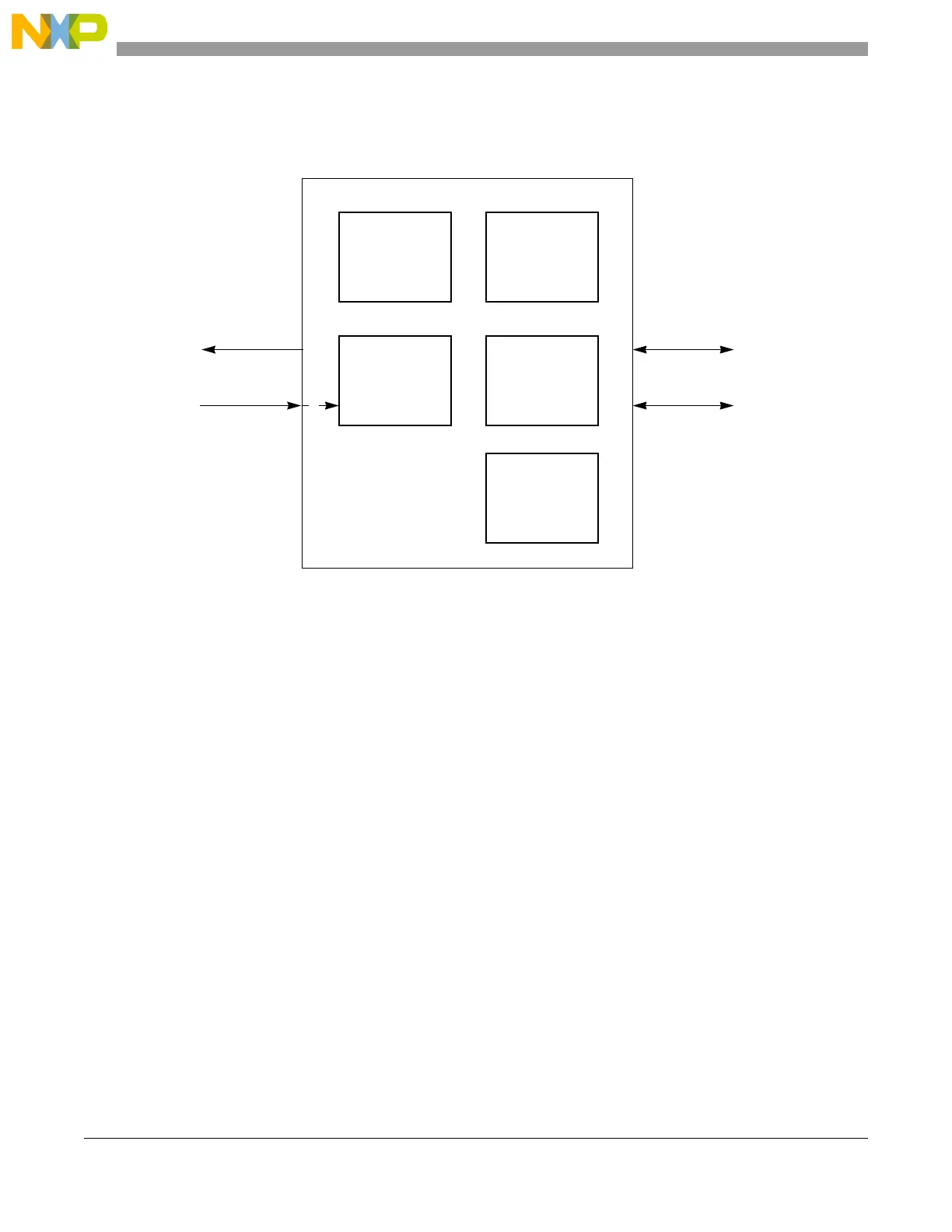
20.1.3 Block diagram
The block diagram of the I
2
C module is shown in Figure 20-1.
Figure 20-1. I
2
C block diagram
20.2 External signal description
The Inter-Integrated Circuit (I
2
C) module has two external pins, SCL and SDA.
20.2.1 SCL
This is the bidirectional Serial Clock Line (SCL) of the module, compatible with the I
2
C-Bus specification.
20.2.2 SDA
This is the bidirectional Serial Data line (SDA) of the module, compatible with the I
2
C-Bus specification.
20.3 Memory map and register description
20.3.1 Module memory map
The memory map for the I
2
C module is given below in Table 20-1. The total address for each register is
the sum of the base address for the I
2
C module and the address offset for each register.
In/Out
Data
Shift
Register
Address
Compare
SDA
Interrupt
Clock
Control
Start
Stop
Arbitration
Control
SCL
bus_clock
I
2
C
Registers