MPC5604B/C Microcontroller Reference Manual, Rev. 8
Freescale Semiconductor 797
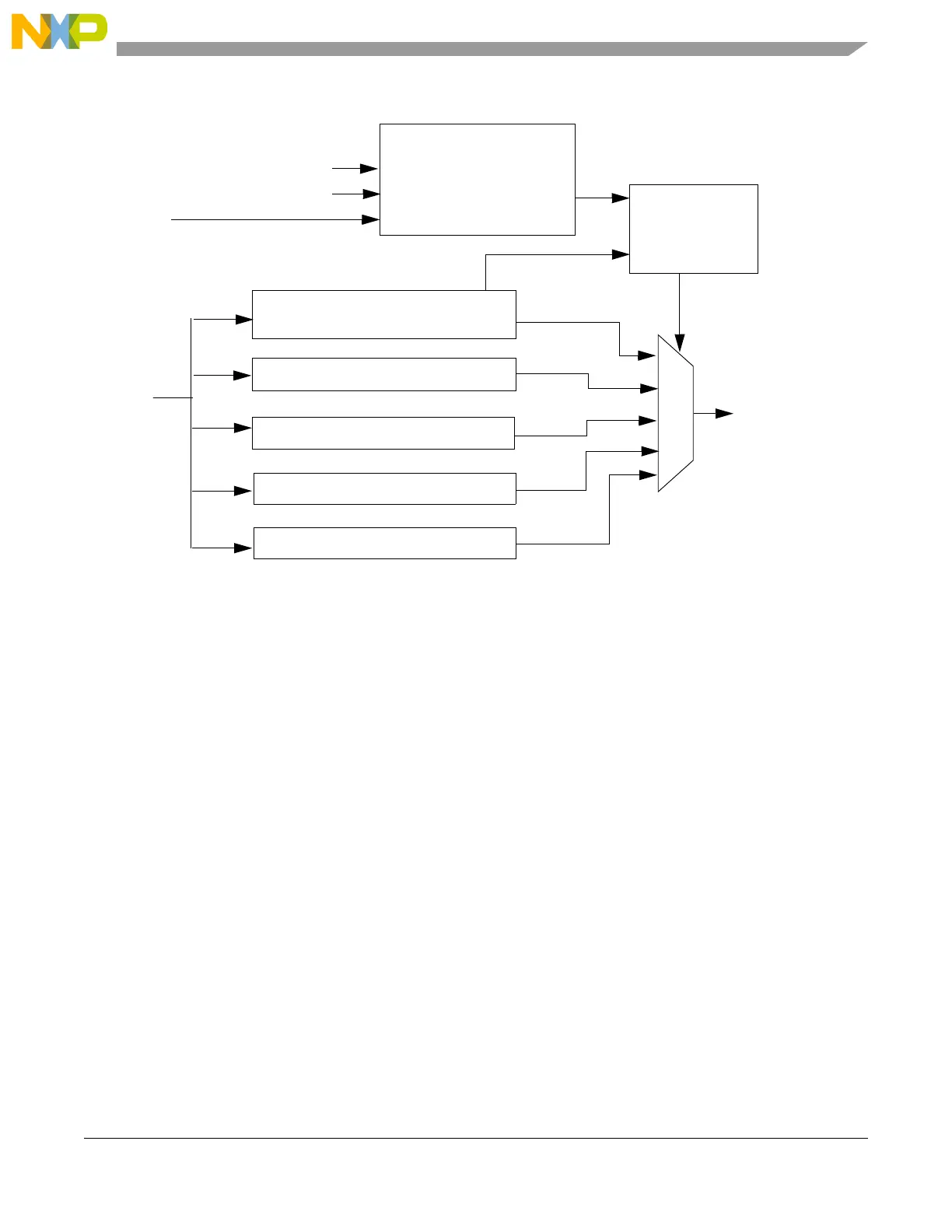
Figure 32-6. e200z0 OnCE Block Diagram
32.9.2 e200z0 OnCE Controller Functional Description
The functional description for the e200z0 OnCE controller is the same as for the JTAGC, with the
differences described below.
32.9.2.1 Enabling the TAP Controller
To access the e200z0 OnCE controller, the proper JTAGC instruction needs to be loaded in the JTAGC
instruction register, as discussed in Section 32.5.2.2, “TAP sharing mode.
32.9.3 e200z0 OnCE Controller Register Description
Most e200z0 OnCE debug registers are fully documented in the e200z0 Reference Manual.
32.9.3.1 OnCE Command Register (OCMD)
The OnCE command register (OCMD) is a 10-bit shift register that receives its serial data from the TDI
pin and serves as the instruction register (IR). It holds the 10-bit commands to be used as input for the
e200z0 OnCE Decoder. The OCMD is shown in Table 32-7. The OCMD is updated when the TAP
controller enters the update-IR state. It contains fields for controlling access to a resource, as well as
controlling single-step operation and exit from OnCE mode.
TCK
e200z0_TMS
TDI
Test Access Port (TAP)
e200z0_TDO
Bypass Register
External Data Register
.
.
Controller
TAP Instruction Register
.
OnCE Mapped Debug Registers
Auxiliary Data Register
.
.
.
e200z0_TRST
(OnCE OCMD)
TDO Mux
Control
{
From
JTAGC
(to JTAGC)