MPC5604B/C Microcontroller Reference Manual, Rev. 8
640 Freescale Semiconductor
• The flash memory core
• The memory interface
The flash memory core is composed of arrayed nonvolatile storage elements, sense amplifiers, row
decoders, column decoders and charge pumps. The arrayed storage elements in the flash memory core are
subdivided into physically separate units referred to as blocks (or sectors).
The memory interface contains the registers and logic which control the operation of the flash memory
core. The memory interface is also the interface between the flash memory module and a platform flash
memory controller. It contains the ECC logic and redundancy logic.
A platform flash memory controller connects the flash memory module to a system bus, and contains all
system level customization required for the device application.
27.2 Main features
27.3 Block diagram
The flash memory module contains one Matrix Module, composed of a single bank (Bank 0) normally
used for code storage. RWW operations are not possible.
Modify operations are managed by an embedded Flash Memory Program/Erase Controller (FPEC).
Commands to the FPEC are given through a User Registers Interface.
The read data bus is 128 bits wide, while the flash memory registers are on a separate bus 32 bits wide
addressed in the user memory map.
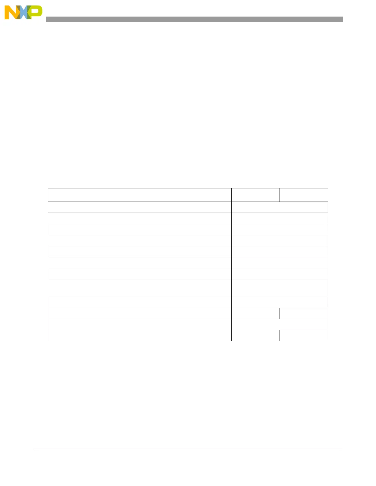
Table 27-1. Flash memory features
Feature CFlash DFlash
High read parallelism (128 bits) Yes
Error Correction Code (SEC-DED) to enhance data retention Yes
Double Word Program (64 bits) Yes
Sector erase Ye s
Single bank—Read-While-Write (RWW) No
Erase Suspend Ye s
Program Suspend No
Software programmable program/erase protection to avoid unwanted
writings
Ye s
Censored Mode against piracy Yes
Shadow Sector available Yes No
One-Time Programmable (OTP) area in Test Flash block Yes
Boot sectors Yes No