MPC5604B/C Microcontroller Reference Manual, Rev. 8
Freescale Semiconductor 503
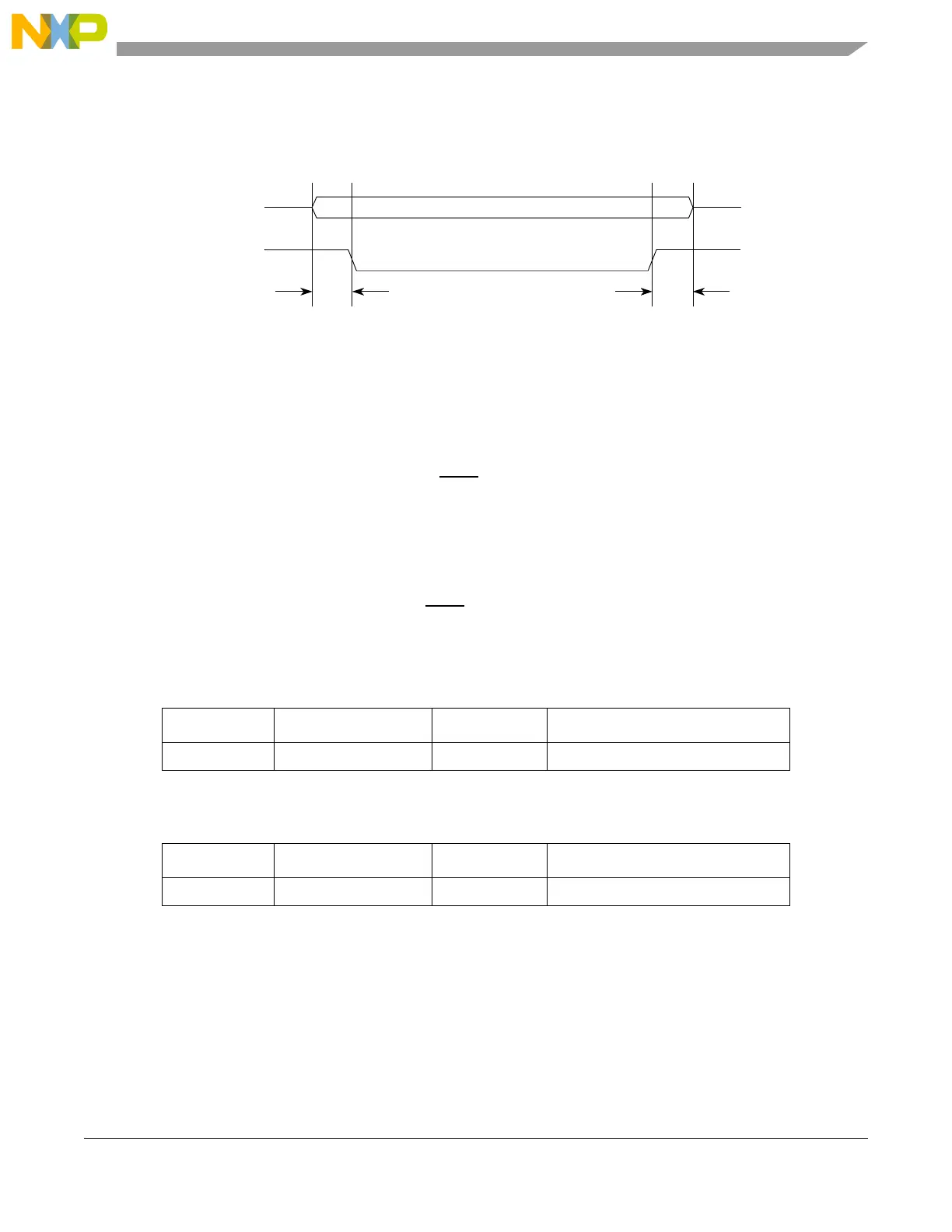
Figure 23-15 shows the timing of the CS5_x signal relative to CS signals.
Figure 23-15. Peripheral chip select strobe timing
The delay between the assertion of the CSx signals and the assertion of CS5_x is selected by the PCSSCK
field in the DSPIx_CTAR based on the following formula:
At the end of the transfer the delay between CS5_x negation and CSx negation is selected by the PASC
field in the DSPIx_CTAR based on the following formula:
Table 23-29 shows an example of the computed t
PCSSCK
delay.
Table 23-30 shows an example of the computed the t
PASC
delay.
23.6.5 Transfer formats
The SPI serial communication is controlled by the serial communications clock (SCK_x) signal and the
CSx signals. The SCK_x signal provided by the master device synchronizes shifting and sampling of the
data by the SIN_x and SOUT_x pins. The CSx signals serve as enable signals for the slave devices.
When the DSPI is the bus master, the CPOL and CPHA bits in the DSPI clock and transfer attributes
registers (DSPIx_CTARn) select the polarity and phase of the serial clock, SCK_x. The polarity bit selects
Table 23-29. Peripheral chip select strobe assert computation example
PCSSCK Prescaler f
SYS
Delay before transfer
0b11 7 64 MHz 109.4 ns
Table 23-30. Peripheral chip select strobe negate computation example
PASC Prescaler f
SYS
Delay after transfer
0b11 7 64 MHz 109.4 ns