MPC5604B/C Microcontroller Reference Manual, Rev. 8
Freescale Semiconductor 43
• Main oscillator pads (EXTAL, XTAL) are tristate.
• Nexus output pads (MDO[n], MCKO, EVTO, MSEO) are forced to output.
4.4 Voltage supply pins
Voltage supply pins are used to provide power to the device. Two dedicated pins are used for 1.2 V
regulator stabilization.
4.5 Pad types
In the device the following types of pads are available for system pins and functional port pins:
S = Slow
1
M = Medium
1
2
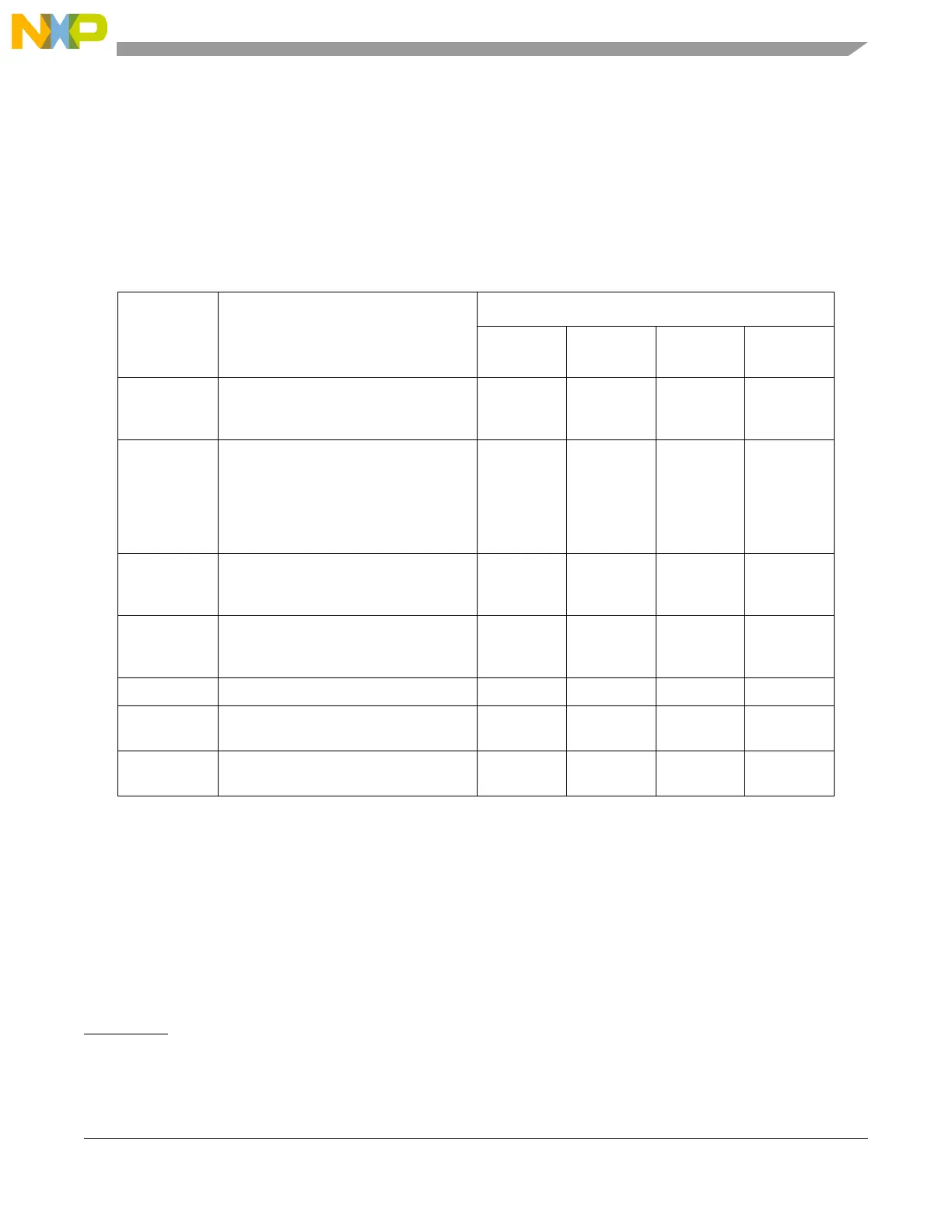
Table 4-1. Voltage supply pin descriptions
Port pin Function
Pin number
64 LQFP
1
1
Pin numbers apply to both the MPC560xB and MPC560xC packages.
100 LQFP 144 LQFP
208
MAPBGA
2
2
208 MAPBGA available only as development package for Nexus2+
VDD_HV Digital supply voltage 7, 28, 56 15, 37, 70,
84
19, 51, 100,
123
C2, D9, E16,
G13, H3, N9,
R5
VSS_HV Digital ground 6, 8, 26, 55 14, 16, 35,
69, 83
18, 20, 49,
99, 122
G7, G8, G9,
G10, H1, H7,
H8, H9, H10,
J7, J8, J9,
J10, K7, K8,
K9, K10
VDD_LV 1.2V decoupling pins. Decoupling
capacitor must be connected between
these pins and the nearest V
SS_LV
pin.
3
3
A decoupling capacitor must be placed between each of the three VDD_LV/VSS_LV supply pairs to ensure stable
voltage (see the recommended operating conditions in the device datasheet for details).
11, 23, 57 19, 32, 85 23, 46, 124 D8, K4, P7
VSS_LV 1.2V decoupling pins. Decoupling
capacitor must be connected between
these pins and the nearest V
DD_LV
pin.
3
10, 24, 58 18, 33, 86 22, 47, 125 C8, J2, N7
VDD_BV Internal regulator supply voltage 12 20 24 K3
VSS_HV_AD
C
Reference ground and analog ground for
the ADC
33 51 73 R15
VDD_HV_AD
C
Reference voltage and analog supply for
the ADC
34 52 74 P14
1. See the I/O pad electrical characteristics in the device datasheet for details.
2. All medium and fast pads are in slow configuration by default at reset and can be configured as fast or medium (see PCR.SRC
in Section 19.5.3.8, “Pad Configuration Registers (PCR0–PCR122)).