MPC5604B/C Microcontroller Reference Manual, Rev. 8
Freescale Semiconductor 121
• contains a set of registers to control clock dividers for divided clock generation
• supports multiple clock sources and maps their address spaces to its memory map
• generates an output clock
• guarantees glitch-less clock transitions when changing the system clock selection
• supports 8-, 16- and 32-bit wide read/write accesses
7.3 Modes of Operation
This section describes the basic functional modes of the MC_CGM.
7.3.1 Normal and Reset Modes of Operation
During normal and reset modes of operation, the clock selection for the system clock is controlled by the
MC_ME.
7.4 External Signal Description
The MC_CGM delivers an output clock to the PA[0] pin for off-chip use and/or observation.
7.5 Memory Map and Register Definition
NOTE
Any access to unused registers as well as write accesses to read-only
registers will:
• not change register content
• cause a transfer error
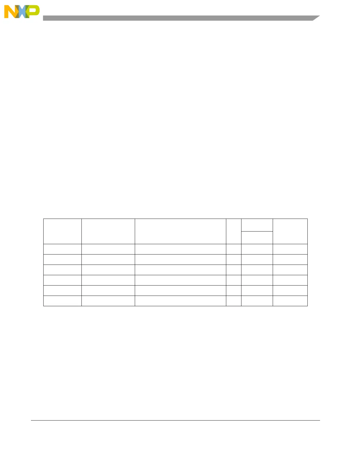
Table 7-1. MC_CGM Register Description
Address Name Description Size
Access
Location
Supervisor
0xC3FE_0370 CGM_OC_EN Output Clock Enable word read/write on page 126
0xC3FE_0374 CGM_OCDS_SC Output Clock Division Select byte read/write on page 126
0xC3FE_0378 CGM_SC_SS System Clock Select Status byte read on page 127
0xC3FE_037C CGM_SC_DC0 System Clock Divider Configuration 0 byte read/write on page 128
0xC3FE_037D CGM_SC_DC1 System Clock Divider Configuration 1 byte read/write on page 128
0xC3FE_037E CGM_SC_DC2 System Clock Divider Configuration 2 byte read/write on page 128
 Loading...