MPC5604B/C Microcontroller Reference Manual, Rev. 8
128 Freescale Semiconductor
7.5.1.4 System Clock Divider Configuration Registers (CGM_SC_DC0…2)
These registers control the system clock dividers.
Table 7-5. System Clock Select Status Register (CGM_SC_SS) Field Descriptions
Field Description
SELSTAT System Clock Source Selection Status — This value indicates the current source for the system clock.
0000 16 MHz int. RC osc.
0001 div. 16 MHz int. RC osc.
0010 4-16 MHz ext. xtal osc.
0011 div. ext. xtal osc.
0100 freq. mod. PLL
0101 reserved
0110 reserved
0111 reserved
1000 reserved
1001 reserved
1010 reserved
1011 reserved
1100 reserved
1101 reserved
1110 reserved
1111 system clock is disabled
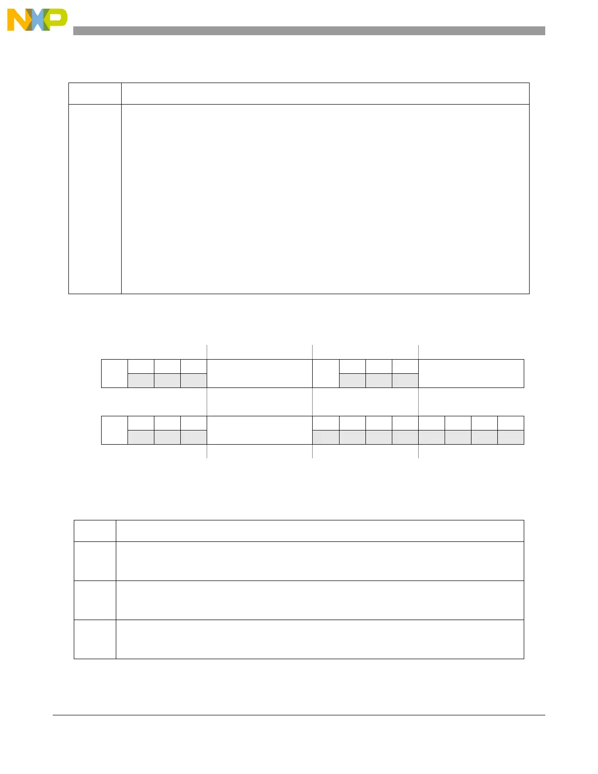
Address 0xC3FE_037C Access: Supervisor read/write
0123456789101112131415
R
DE0
000
DIV0 DE1
000
DIV1
W
Reset1000000010000000
16 17 18 19 20 21 22 23 24 25 26 27 28 29 30 31
R
DE2
000
DIV2
00000000
W
Reset1000000000000000
Figure 7-5. System Clock Divider Configuration Registers (CGM_SC_DC0…2)
Table 7-6. System Clock Divider Configuration Registers (CGM_SC_DC0…2) Field Descriptions
Field Description
DE0 Divider 0 Enable
0 Disable system clock divider 0
1 Enable system clock divider 0
DIV0 Divider 0 Division Value — The resultant peripheral set 1 clock will have a period DIV0 + 1 times that of
the system clock. If the DE0 is set to ‘0’ (Divider 0 is disabled), any write access to the DIV0 field is ignored
and the peripheral set 1 clock remains disabled.
DE1 Divider 1 Enable
0 Disable system clock divider 1
1 Enable system clock divider 1
 Loading...