MPC5604B/C Microcontroller Reference Manual, Rev. 8
494 Freescale Semiconductor
23.6 Functional description
The DSPI supports full-duplex, synchronous serial communications between the MCU and peripheral
devices. All communications are through an SPI-like protocol.
The DSPI has one configuration, namely serial peripheral interface (SPI), in which the DSPI operates as
a basic SPI or a queued SPI.
The DCONF field in the DSPIx_MCR register determines the DSPI configuration. See Table 23-3 for the
DSPI configuration values.
The DSPIx_CTAR0–DSPIx_CTAR5 registers hold clock and transfer attributes.The SPI configuration can
select which CTAR to use on a frame by frame basis by setting the CTAS field in the DSPIx_PUSHR.
The 16-bit shift register in the master and the 16-bit shift register in the slave are linked by the SOUT_x
and SIN_x signals to form a distributed 32-bit register. When a data transfer operation is performed, data
is serially shifted a pre-determined number of bit positions. Because the registers are linked, data is
exchanged between the master and the slave; the data that was in the master’s shift register is now in the
shift register of the slave, and vice versa. At the end of a transfer, the TCF bit in the DSPIx_SR is set to
indicate a completed transfer. Figure 23-12 illustrates how master and slave data is exchanged.
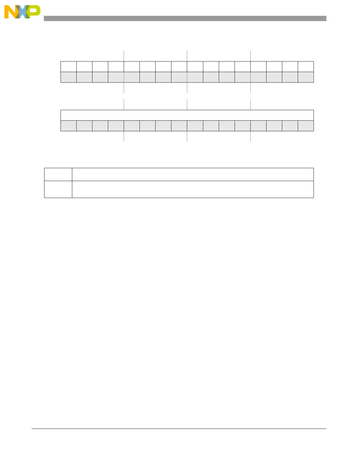
Offsets: 0x7C–0x88 (4 registers) Access: Read
0123456789101112131415
R0000000000000000
W
Reset0000000000000000
16 17 18 19 20 21 22 23 24 25 26 27 28 29 30 31
RRXDATA
W
Reset0000000000000000
Figure 23-11. DSPI Receive FIFO Registers 0–3 (DSPIx_RXFRn)
Table 23-23. DSPIx_RXFRn field description
Field Description
RXDATA Receive data
Contains the received SPI data.