MPC5604B/C Microcontroller Reference Manual, Rev. 8
104 Freescale Semiconductor
6.7.5 Register description
The FMPLL operation is controlled by two registers. Those registers can be accessed and written in
supervisor mode only.
6.7.5.1 Control Register (CR)
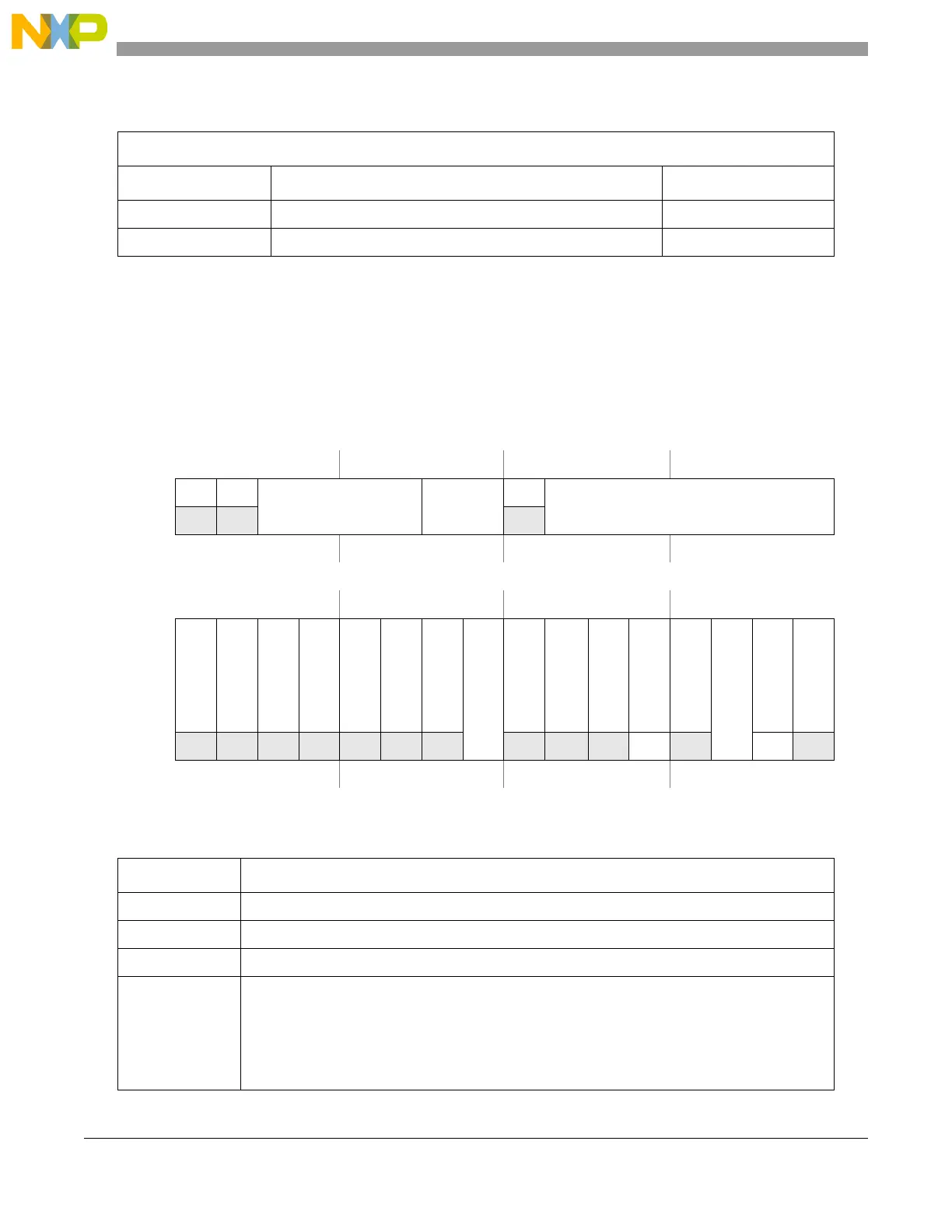
Table 6-8. FMPLL memory map
Base address: 0xC3FE_00A0
Address offset Register Location
0x0 Control Register (CR) on page 104
0x4 Modulation Register (MR) on page 106
Offset: 0x0 Access: Supervisor read/write
0123456789101112131415
R 0 0
IDF ODF
0
NDIV
W
Reset0000001001000000
16 17 18 19 20 21 22 23 24 25 26 27 28 29 30 31
R
0000000
EN_PLL_SW
0
UNLOCK_ONCE
0
I_LOCK
S_LOCK
PLL_FAIL_MASK
PLL_FAIL_FLAG
1
W
w1c w1c
Reset0000000000000001
Figure 6-7. Control Register (CR)
Table 6-9. CR field descriptions
Field Description
IDF The value of this field sets the FMPLL input division factor as described in Ta bl e 6 -10.
ODF The value of this field sets the FMPLL output division factor as described in Table 6-11.
NDIV The value of this field sets the FMPLL loop division factor as described in Tabl e 6-12.
EN_PLL_SW This bit is used to enable progressive clock switching. After the PLL locks, the PLL output initially
is divided by 8, and then progressively decreases until it reaches divide-by-1.
0 Progressive clock switching disabled.
1 Progressive clock switching enabled.
Note: Progressive clock switching should not be used if a non-changing clock is needed, such
as for serial communications, until the division has finished.