MPC5604B/C Microcontroller Reference Manual, Rev. 8
648 Freescale Semiconductor
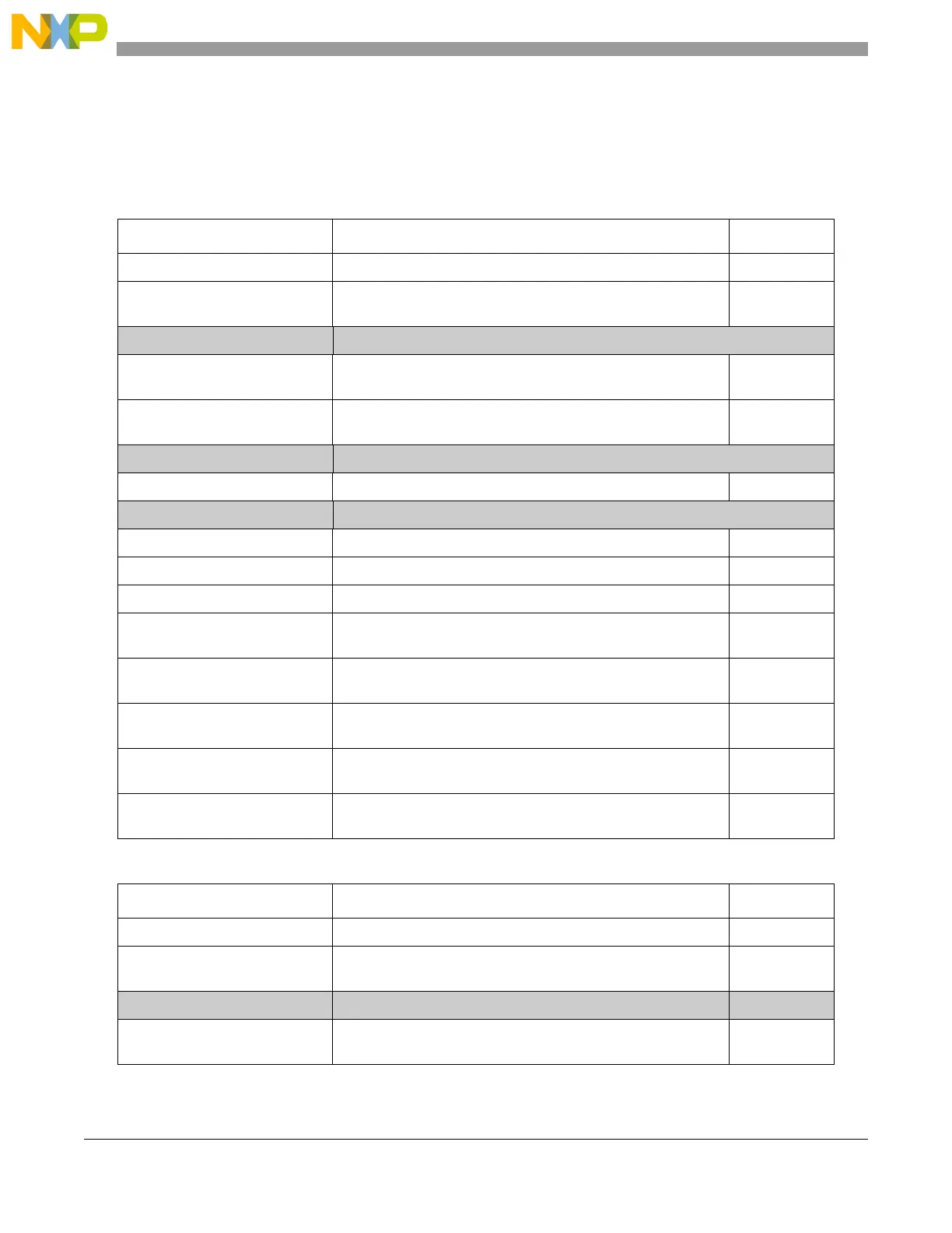
27.5 Register description
The CFlash and DFlash modules have respective sets of memory mapped registers. The CFlash register
mapping is shown in Table 27-7. The DFlash register mapping is shown in Table 27-8.
Table 27-7. CFlash registers
Address offset Register Location
0x0000 CFlash Module Configuration Register (CFLASH_MCR) on page 649
0x0004 CFlash Low/Mid Address Space Block Locking Register
(CFLASH_LML)
on page 655
0x0008 Reserved
0x000C CFlash Secondary Low/Mid Address Space Block Locking
Register (CFLASH_SLL)
on page 659
0x0010 CFlash Low/Mid Address Space Block Select Register
(CFLASH_LMS)
on page 665
0x0014 Reserved
0x0018 CFlash Address Register (CFLASH_ADR) on page 666
0x0028–0x0038 Reserved
0x003C CFlash User Test 0 register (CFLASH_UT0) on page 667
0x0040 CFlash User Test 1 register (CFLASH_UT1) on page 669
0x0044 CFlash User Test 2 register (CFLASH_UT2) on page 669
0x0048 CFlash User Multiple Input Signature Register 0
(CFLASH_UMISR0)
on page 670
0x004C CFlash User Multiple Input Signature Register 1
(CFLASH_UMISR1)
on page 671
0x0050 CFlash User Multiple Input Signature Register 2
(CFLASH_UMISR2)
on page 672
0x0054 CFlash User Multiple Input Signature Register 3
(CFLASH_UMISR3)
on page 673
0x0058 CFlash User Multiple Input Signature Register 4
(CFLASH_UMISR4)
on page 674
Table 27-8. DFlash registers
Address offset Register name Location
0x0000 DFlash Module Configuration Register (DFLASH_MCR) on page 680
0x0004 DFlash Low/Mid Address Space Block Locking Register
(DFLASH_LML)
on page 685
0x0008 Reserved —
0x000C DFlash Secondary Low/Mid Address Space Block Locking
Register (DFLASH_SLL)
on page 689